 ChipApex | Global Electronic Components Supplier

SEARCH
Search Product
Search Post
— IC芯片 | 连接器 | 传感器 | 被动器件 —
Search productSearch post
— IC芯片 | 连接器 | 传感器 | 被动器件 —
Consult the customer manager about the wholesale price.
consultation hotline:86-132-6715-2157
email:[email protected]
Contact the product manager for consultation. One-stop consultation is available.
Do you want a lower wholesale price? Please send us your inquiry and we will reply immediately.
The CDCBT1001DPWR is a single-channel clock buffer and driver manufactured by Texas Instruments. It operates with an LVCMOS input and provides a corresponding LVCMOS output, configured for a 1:1 signal ratio. The device supports a maximum operating frequency of 24 MHz and functions within a supply voltage range of 1.08 V to 1.32 V. Designed for surface-mount applications, it is housed in a compact 5-X2SON package measuring 0.8 mm by 0.8 mm with an exposed pad. The component is rated for an ambient operating temperature range from -40°C to +85°C.
Verify the specific ordering suffix to confirm packaging configuration, as the part is available in both Tape & Reel and Cut Tape formats. Ensure the design accommodates the specified 1.08 V to 1.32 V supply voltage range and the thermal requirements of the 5-X2SON package with an exposed pad for proper heat dissipation during operation.
Select this component when a single-ended LVCMOS clock signal requires buffering without inversion or differential conversion. The 24 MHz frequency limit defines its suitability for lower-speed digital circuits. Designers must ensure the power supply remains strictly within the 1.08 V to 1.32 V window to maintain correct logic levels and operational stability across the industrial temperature range.
This device belongs to the clock buffer and driver category within Texas Instruments' portfolio. It serves as a standalone solution for distributing clock signals in space-constrained designs. The 5-X2SON package offers a small form factor compared to traditional leaded packages, facilitating high-density PCB layouts for modern consumer and industrial electronics.
Check for pin-compatible alternatives within the same family that may offer different voltage ranges or higher frequency capabilities if system requirements change. Verify that any substitute maintains the LVCMOS input/output specification and fits the 5-X2SON footprint.
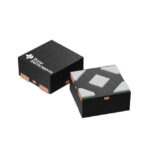 CDCBT1001DPWR

The activity of extra discounts on wholesale prices is in full swing…
Please fill in your contact information and we will send you the latest wholesale price list.






