 ChipApex | Global Electronic Components Supplier

SEARCH
Search Product
Search Post
— IC芯片 | 连接器 | 传感器 | 被动器件 —
Search productSearch post
— IC芯片 | 连接器 | 传感器 | 被动器件 —
Consult the customer manager about the wholesale price.
consultation hotline:86-132-6715-2157
email:[email protected]
Contact the product manager for consultation. One-stop consultation is available.
Do you want a lower wholesale price? Please send us your inquiry and we will reply immediately.
The CDCDB2000ENPPR is a DB2000QL-compliant clock buffer featuring one circuit with a 1:20 input-to-output ratio. It supports differential HCSL input and output signals, operating at a maximum frequency of 250 MHz. The device functions within a supply voltage range of 3.135 V to 3.465 V and is rated for an ambient temperature range of -40°C to 85°C. Packaged in an 80-TLGA (6x6) surface-mount case with an exposed pad, it is supplied in Tape & Reel format.
Verify the specific ordering suffix ENPPR corresponds to the Tape & Reel packaging configuration. Confirm that the 80-TLGA footprint matches the target PCB design requirements. Ensure the 3.135 V to 3.465 V supply voltage range aligns with the system power rails. Check for any additional qualification or reliability data required for the specific deployment environment.
Select this component when a single differential HCSL source must drive twenty downstream HCSL loads. The 250 MHz frequency limit suits standard PCIe generation clock rates. The wide supply voltage tolerance allows flexibility in power delivery design. The TLGA package requires careful thermal management due to the exposed pad structure.
This part belongs to Texas Instruments' CDCDB series of clock buffers designed for high-speed serial interface standards. It serves as a fan-out buffer specifically optimized for the electrical requirements of PCI Express specifications. The device replaces discrete buffering solutions to reduce board space and signal integrity issues in complex multi-lane systems.
The CDCDB2000ENPPR is functionally compatible with other variants in the CDCDB2000 family, such as the CDCDB2000NPPT. Verify pinout compatibility and package dimensions before substituting different suffixes within the same series.
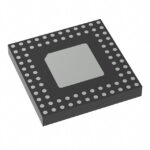 CDCDB2000ENPPR

The activity of extra discounts on wholesale prices is in full swing…
Please fill in your contact information and we will send you the latest wholesale price list.





