 ChipApex | Global Electronic Components Supplier

SEARCH
Search Product
Search Post
— IC芯片 | 连接器 | 传感器 | 被动器件 —
Search productSearch post
— IC芯片 | 连接器 | 传感器 | 被动器件 —
Consult the customer manager about the wholesale price.
consultation hotline:86-132-6715-2157
email:[email protected]
Contact the product manager for consultation. One-stop consultation is available.
Do you want a lower wholesale price? Please send us your inquiry and we will reply immediately.
The CDCDB400RHBT is a DB800ZL-compliant 4-output LP-HCSL clock buffer designed for PCIe Gen 1 through Gen 7, QPI, UPI, SAS, and SATA interfaces. It operates on a single 3V to 3.6V supply with a maximum frequency of 250 MHz. The device features programmable integrated differential output terminations (default 85Ω or selectable 100Ω), hardware-controlled low power mode, and SMBus configuration. Additive phase jitter ranges from 11.3fs RMS (PCIe Gen 7) to 38fs RMS (DB2000Q filter). It supports common clock and individual reference architectures in a 32-pin VQFN package.
Verify the specific suffix RHBT corresponds to the Tape & Reel packaging format as indicated in the product parameters. Confirm that the component meets the required operating temperature range of -40°C to 105°C for the target application environment. Ensure compatibility with the 3.3V core and IO supply voltages specified in the datasheet.
Select this component when a low-jitter, DB800ZL-compliant buffer is required for high-speed serial interfaces like PCIe Gen 1-7. The choice depends on the need for integrated 85Ω/100Ω termination and SMBus configurability. Verify that the 32-VQFN package dimensions fit the PCB layout constraints and that the thermal resistance metrics are sufficient for the expected power dissipation.
The CDCDB400 is a derivative of the DB800ZL specification, meeting or exceeding its system parameters. It also complies with the DB2000Q specification. This positioning allows it to serve as a direct replacement or upgrade in designs originally targeting those Intel specifications for reference clock distribution.
Public confirmed substitute part numbers are not available in the provided documentation.
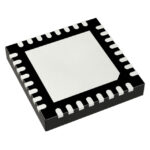 CDCDB400RHBT

The activity of extra discounts on wholesale prices is in full swing…
Please fill in your contact information and we will send you the latest wholesale price list.





