 ChipApex | Global Electronic Components Supplier

SEARCH
Search Product
Search Post
— IC芯片 | 连接器 | 传感器 | 被动器件 —
Search productSearch post
— IC芯片 | 连接器 | 传感器 | 被动器件 —
Consult the customer manager about the wholesale price.
consultation hotline:86-132-6715-2157
email:[email protected]
Contact the product manager for consultation. One-stop consultation is available.
Do you want a lower wholesale price? Please send us your inquiry and we will reply immediately.
The CDCLVC1102PWR is a low jitter, 1:2 LVCMOS fan-out clock buffer manufactured by Texas Instruments. It operates within a supply voltage range of 2.3 V to 3.6 V and supports maximum input and output frequencies of 250 MHz. The device features a propagation delay of up to 2 ns and utilizes LVCMOS logic levels for both input and output signals. Packaged in an 8-TSSOP surface-mount case with dimensions of 4.40 mm width, it is designed for applications requiring reliable clock distribution. The component functions as a single-circuit fanout buffer without differential signaling capabilities.
Verify the specific packaging configuration required for production, as the CDCLVC1102PWR is available in both Tape & Reel (TR) and Cut Tape (CT) formats. Confirm that the 8-TSSOP footprint matches the PCB design constraints. Ensure the selected variant meets the -40°C to +85°C operating temperature range necessary for the intended environment. Cross-reference the manufacturer part number with distributor catalogs to ensure compatibility with existing inventory systems.
Select this component when a single-input, dual-output LVCMOS clock buffer is required for frequencies up to 250 MHz. The 2.3 V to 3.6 V supply range accommodates standard 3.3 V and 2.5 V logic systems. Consider the 8-TSSOP package size for space-constrained surface-mount designs. Compare against other members of the CDCLVC11xx series if higher fan-out ratios such as 1:3 or 1:4 are needed instead.
This device belongs to the CDCLVC11xx family of modular, high-performance, low-skew universal clock buffers from Texas Instruments. The series includes variants with different output counts, ranging from 1:2 to 1:12, all sharing pin-to-pin compatibility. This specific model represents the lowest fan-out option in the lineup, providing two outputs from a single LVCMOS input source.
Pin-compatible alternatives within the same family include CDCLVC1103PW, CDCLVC1104PWR, and CDCLVC1106PWR. These parts offer higher output counts while maintaining identical electrical characteristics and package footprints. Verify that the increased drive capability of higher-count buffers does not exceed power budget constraints.
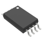 CDCLVC1102PWR

The activity of extra discounts on wholesale prices is in full swing…
Please fill in your contact information and we will send you the latest wholesale price list.




