 ChipApex | Global Electronic Components Supplier

SEARCH
Search Product
Search Post
— IC芯片 | 连接器 | 传感器 | 被动器件 —
Search productSearch post
— IC芯片 | 连接器 | 传感器 | 被动器件 —
Consult the customer manager about the wholesale price.
consultation hotline:86-132-6715-2157
email:[email protected]
Contact the product manager for consultation. One-stop consultation is available.
Do you want a lower wholesale price? Please send us your inquiry and we will reply immediately.
The CDCLVC1106PW is a low jitter, 1:6 LVCMOS fan-out clock buffer manufactured by Texas Instruments. It operates within a supply voltage range of 2.3 V to 3.6 V and supports maximum input and output frequencies of 250 MHz. The device features a propagation delay of up to 2 ns and utilizes an LVCMOS input type. It is housed in a 14-TSSOP package with a width of 4.40 mm. The component functions as a single-circuit fanout buffer without differential inputs or outputs, designed for surface mount installation.
Verify the specific ordering suffix 'PW' corresponds to the tube packaging configuration rather than tape-and-reel variants like 'PWR'. Confirm that the 14-TSSOP physical dimensions match the design footprint requirements. Ensure the 2.3 V to 3.6 V supply voltage range aligns with the target system power rails before finalizing procurement specifications.
Select this component when a single-ended LVCMOS clock signal requires splitting into six distinct paths. The 1:6 ratio distinguishes it from other family members such as the CDCLVC1102 (1:2) or CDCLVC1108 (1:8). Consider the 250 MHz frequency limit and 2 ns delay characteristics against system timing constraints. The 14-TSSOP package offers a compact solution for space-constrained PCB layouts.
This part belongs to the CDCLVC11xx series of modular, high-performance, low-skew universal clock buffers. The series includes variants with different output counts, ranging from 1:2 to 1:12, all sharing pin-to-pin compatibility. This modularity allows designers to substitute equivalent parts within the same family based on specific fan-out requirements while maintaining consistent electrical performance and package footprints.
Compatible substitutes include CDCLVC1102PW, CDCLVC1103PW, CDCLVC1104PW, CDCLVC1108PW, CDCLVC1110PW, and CDCLVC1112PW due to shared pinouts and electrical characteristics.
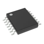 CDCLVC1106PW

The activity of extra discounts on wholesale prices is in full swing…
Please fill in your contact information and we will send you the latest wholesale price list.





