 ChipApex | Global Electronic Components Supplier

SEARCH
Search Product
Search Post
— IC芯片 | 连接器 | 传感器 | 被动器件 —
Search productSearch post
— IC芯片 | 连接器 | 传感器 | 被动器件 —
Consult the customer manager about the wholesale price.
consultation hotline:86-132-6715-2157
email:[email protected]
Contact the product manager for consultation. One-stop consultation is available.
Do you want a lower wholesale price? Please send us your inquiry and we will reply immediately.
The CDCLVC1108PW is a low jitter, 1:8 LVCMOS fan-out clock buffer manufactured by Texas Instruments. It operates within a supply voltage range of 2.3 V to 3.6 V and supports maximum input and output frequencies of 250 MHz. The device features a propagation delay of up to 2 ns and consumes approximately 10 mA of operating current. Packaged in a 16-TSSOP surface-mount case with a width of 4.40 mm, it functions reliably across an industrial temperature range of -40°C to +85°C.
Verify the package type matches the required 16-TSSOP form factor. Confirm that the supply voltage requirements align with the 2.3 V to 3.6 V operational range. Ensure the design accommodates the specified -40°C to +85°C temperature limits for the target environment.
Select this component when an 8-channel LVCMOS clock distribution is required. Compare against other CDCLVC11xx variants if different fan-out ratios such as 1:2 or 1:6 are needed. Ensure the PCB layout allows for proper decoupling near the power pins to maintain signal integrity at 250 MHz.
This part belongs to the CDCLVC11xx modular clock buffer series from Texas Instruments. The family includes variants with 1:2 through 1:12 outputs, all sharing pin compatibility and core electrical characteristics. This specific model provides the 1:8 configuration within the standard TSSOP packaging options available for the series.
Other models in the CDCLVC11xx series, such as CDCLVC1102, CDCLVC1103, CDCLVC1104, CDCLVC1106, CDCLVC1110, and CDCLVC1112, are pin-compatible alternatives offering different output counts.
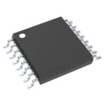 CDCLVC1108PW

The activity of extra discounts on wholesale prices is in full swing…
Please fill in your contact information and we will send you the latest wholesale price list.






