 ChipApex | Global Electronic Components Supplier

SEARCH
Search Product
Search Post
— IC芯片 | 连接器 | 传感器 | 被动器件 —
Search productSearch post
— IC芯片 | 连接器 | 传感器 | 被动器件 —
Consult the customer manager about the wholesale price.
consultation hotline:86-132-6715-2157
email:[email protected]
Contact the product manager for consultation. One-stop consultation is available.
Do you want a lower wholesale price? Please send us your inquiry and we will reply immediately.
The CDCLVD110VFG4 is a low skew clock buffer and distribution multiplexer manufactured by Texas Instruments. It features a 2:10 input-to-output ratio with differential LVDS inputs and outputs, supporting maximum frequencies up to 1.1 GHz. The device operates within a supply voltage range of 2.375 V to 2.625 V and functions across an industrial temperature range of -40°C to +85°C. Packaged in a 32-LQFP (7x7 mm) surface-mount case, it is designed for high-performance clock distribution applications requiring minimal skew.
Verify the specific package variant against the datasheet, as the 'G4' suffix typically indicates lead-free status but does not alter electrical function. Confirm the 32-LQFP footprint dimensions match the PCB layout requirements. Ensure the design accommodates the specified 2.375 V to 2.625 V supply voltage constraints for proper operation.
Select this component when a 2:10 differential LVDS fanout is required with a maximum frequency of 1.1 GHz. It is suitable for designs needing a single-circuit multiplexer with low skew characteristics. Ensure the system power supply can be regulated strictly between 2.375 V and 2.625 V to meet the operational specifications.
This part belongs to the CDCLVD110 family of low skew clock buffers. It serves as a specialized solution for distributing differential LVDS clock signals in complex digital systems. The device integrates multiplexing capabilities to select between multiple input sources while maintaining signal integrity across ten output channels.
Check for pin-compatible alternatives within the same Texas Instruments family that offer similar LVDS specifications. Verify if other variants provide different packaging options or extended temperature ranges if the current selection does not meet environmental constraints.
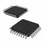 CDCLVD110VFG4

The activity of extra discounts on wholesale prices is in full swing…
Please fill in your contact information and we will send you the latest wholesale price list.





