 ChipApex | Global Electronic Components Supplier

SEARCH
Search Product
Search Post
— IC芯片 | 连接器 | 传感器 | 被动器件 —
Search productSearch post
— IC芯片 | 连接器 | 传感器 | 被动器件 —
Consult the customer manager about the wholesale price.
consultation hotline:86-132-6715-2157
email:[email protected]
Contact the product manager for consultation. One-stop consultation is available.
Do you want a lower wholesale price? Please send us your inquiry and we will reply immediately.
The CDCLVD1208RHDT is a low-additive-jitter LVDS clock buffer manufactured by Texas Instruments. It distributes one of two selectable clock inputs to eight differential LVDS outputs with minimal skew. The device supports LVCMOS, LVDS, and LVPECL input protocols and operates on a single 2.5V supply (2.375V to 2.625V). Key electrical parameters include a maximum output frequency of 800 MHz, a maximum propagation delay of 600 ps, and an RMS additive jitter of less than 300 fs from 10 kHz to 20 MHz. It is housed in a 28-pin VQFN package.
Verify the suffix RHDT corresponds to the Tape & Reel packaging configuration as indicated by the supplier data. Confirm that the 28-VQFN (5x5) package dimensions align with the PCB footprint requirements. Ensure the 2.375V to 2.625V supply voltage range matches the system power design. Check for moisture sensitivity level requirements during storage and handling.
Select this component when driving multiple LVDS loads from a single or dual clock source with strict jitter constraints. The 800 MHz maximum frequency limits its use compared to higher-speed variants like the LMK1D1208. Verify compatibility between the input signal protocol (LVDS/LVPECL/LVCMOS) and the source driver. The fixed 2.5V supply requirement simplifies power management but restricts multi-voltage domain integration.
This part belongs to the CDCLVD series of low-power, low-jitter clock buffers. It serves as a fanout buffer and multiplexer, allowing selection between two input sources. It is distinct from the I2C-programmable LMK1D1208I, which offers configurable output amplitudes and addresses. The CDCLVD1208 provides hardware-controlled input selection via the IN_SEL pin.
The CDCLVD1208RHDT is functionally equivalent to the CDCLVD1208RHD. Other family members such as CDCLVD1204 (4 outputs) or CDCLVD1212 (12 outputs) offer different fanout ratios. Higher-performance alternatives include the LMK1D1208 series for frequencies up to 2 GHz.
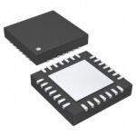 CDCLVD1208RHDT

The activity of extra discounts on wholesale prices is in full swing…
Please fill in your contact information and we will send you the latest wholesale price list.






