 ChipApex | Global Electronic Components Supplier

SEARCH
Search Product
Search Post
— IC芯片 | 连接器 | 传感器 | 被动器件 —
Search productSearch post
— IC芯片 | 连接器 | 传感器 | 被动器件 —
Consult the customer manager about the wholesale price.
consultation hotline:86-132-6715-2157
email:[email protected]
Contact the product manager for consultation. One-stop consultation is available.
Do you want a lower wholesale price? Please send us your inquiry and we will reply immediately.
The CDCLVP1208RHDR is a high-performance clock buffer manufactured by Texas Instruments, featuring an 8-output LVPECL fanout configuration. It accepts differential or single-ended inputs including LVPECL, LVDS, and LVCMOS/LVTTL through a selectable multiplexer controlled by the IN_SEL pin. The device supports maximum clock frequencies up to 2 GHz with a maximum propagation delay of 450 ps. Powered by a 2.375 V to 3.6 V supply, it delivers low additive jitter (less than 100 fs RMS from 10 kHz to 20 MHz) and minimal output skew of 20 ps. Packaged in a 28-pin VQFN (5 mm x 5 mm), it operates within an industrial temperature range of -40°C to +85°C.
Verify that the ordering suffix RHDR corresponds to the Tape & Reel packaging format as specified in the datasheet. Confirm the component grade matches industrial requirements (-40°C to +85°C). Ensure the supplier provides documentation confirming the RoHS compliance status and lead-free manufacturing process for this specific part number.
Select the CDCLVP1208RHDR when driving multiple LVPECL loads with strict timing constraints. Ensure the design accommodates the 2.375 V to 3.6 V supply voltage range. Verify that the PCB layout supports the exposed thermal pad for adequate heat dissipation, as the junction-to-pad thermal resistance is critical for maintaining performance at higher temperatures.
This component belongs to the CDCLVP series of low-power, low-jitter clock buffers. It serves as a distribution element for converting universal input clock signals into eight synchronized LVPECL outputs. The RHDR suffix indicates the specific tape-and-reel packaging variant designed for automated surface-mount assembly processes.
Direct replacements within the same family include CDCLVP1204 (4 outputs) and CDCLVP2104 (dual 1:4 buffers). For identical 8-output functionality, verify compatibility with CDCLVP1208 variants differing only in package or reel specifications.
Input selection is managed by the IN_SEL pin. A logic low selects the INP0/INN0 pair, while a logic high selects the INP1/INN1 pair.
The recommended termination is a 50 Ω resistor connected to (VCC - 2) V. AC coupling is required if the driver and receiver operate on different supply voltages.
Yes, unused differential input pairs can be left floating without affecting the operation of the active inputs.
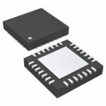 CDCLVP1208RHDR

The activity of extra discounts on wholesale prices is in full swing…
Please fill in your contact information and we will send you the latest wholesale price list.





