 ChipApex | Global Electronic Components Supplier

SEARCH
Search Product
Search Post
— IC芯片 | 连接器 | 传感器 | 被动器件 —
Search productSearch post
— IC芯片 | 连接器 | 传感器 | 被动器件 —
Consult the customer manager about the wholesale price.
consultation hotline:86-132-6715-2157
email:[email protected]
Contact the product manager for consultation. One-stop consultation is available.
Do you want a lower wholesale price? Please send us your inquiry and we will reply immediately.
The CDCLVP1208RHDT is a low additive jitter, high-performance clock buffer manufactured by Texas Instruments. It features an internal multiplexer that selects one of two differential or single-ended inputs (LVPECL, LVDS, or LVCMOS/LVTTL) to drive eight differential LVPECL outputs. The device supports maximum clock frequencies up to 2 GHz with a maximum propagation delay of 450 ps and output skew as low as 20 ps. It operates on a supply voltage range of 2.375 V to 3.6 V, consuming a maximum core current of 73 mA. Packaged in a 28-pin QFN (5 mm x 5 mm), it is characterized for industrial temperatures from -40°C to +85°C.
Verify the specific ordering suffix RHDT corresponds to the Tape & Reel packaging configuration. Confirm the component grade matches the standard industrial temperature range (-40°C to +85°C). Ensure the package body size is identified as the 28-VFQFN Exposed Pad variant.
Select this component when driving multiple LVPECL loads from a single source requiring minimal skew. Verify input signal compatibility with the supported LVPECL, LVDS, or LVCMOS/LVTTL formats. Ensure the system power supply falls within the 2.375 V to 3.6 V operating range and thermal management accommodates the specified junction-to-ambient resistance.
This part belongs to the CDCLVP series of clock buffers. It provides a 2-input to 8-output distribution architecture designed for high-speed clocking applications. The RHD suffix indicates the specific 28-pin QFN package type used for surface mount assembly.
Consult official documentation for verified substitute part numbers. Do not assume functional equivalence with other buffer families without verifying electrical parameters and pinout compatibility.
The CDCLVP1208 accepts LVPECL, LVDS, and LVCMOS/LVTTL inputs through its two selectable input pairs.
Input selection is controlled via the IN_SEL pin. A logic level of 0 selects the INP0/INN0 pair, while a logic level of 1 selects the INP1/INN1 pair.
The overall additive jitter is less than 100 fs RMS in the 10 kHz to 20 MHz offset range, with typical values of 57 fs at 122.88 MHz and 30 fs at 312.5 MHz.
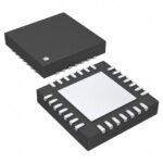 CDCLVP1208RHDT

The activity of extra discounts on wholesale prices is in full swing…
Please fill in your contact information and we will send you the latest wholesale price list.






