 ChipApex | Global Electronic Components Supplier

SEARCH
Search Product
Search Post
— IC芯片 | 连接器 | 传感器 | 被动器件 —
Search productSearch post
— IC芯片 | 连接器 | 传感器 | 被动器件 —
Consult the customer manager about the wholesale price.
consultation hotline:86-132-6715-2157
email:[email protected]
Contact the product manager for consultation. One-stop consultation is available.
Do you want a lower wholesale price? Please send us your inquiry and we will reply immediately.
The CDCLVP2102RGTT is a low-jitter dual 1:2 universal-to-LVPECL clock buffer manufactured by Texas Instruments. It accepts LVPECL, LVDS, or LVCMOS/LVTTL inputs and provides four differential LVPECL outputs. The device supports a maximum clock frequency of 2 GHz with a supply voltage range of 2.375 V to 3.6 V. Key electrical specifications include a maximum propagation delay of 450 ps and an additive jitter of less than 100 fs RMS within the 10 kHz to 20 MHz offset range. It operates within an industrial temperature range of -40°C to +85°C and is housed in a 16-VQFN (3x3 mm) package.
Verify the specific ordering suffix against the manufacturer's official datasheet to confirm package type and reel specifications. Ensure the selected variant matches the required tape and reel quantity for manufacturing integration. Cross-reference the RoHS compliance status and humidity sensitivity classification prior to procurement to meet storage and handling requirements.
Select this component when driving multiple LVPECL loads from diverse input standards such as LVDS or LVCMOS. The device is suitable for designs requiring minimal added jitter below 100 fs RMS. Verify that the system power supply remains within the 2.375 V to 3.6 V range and that the PCB layout accommodates the 16-VQFN exposed pad thermal requirements for reliable operation at frequencies up to 2 GHz.
This part belongs to the CDCLVP family of low-voltage positive emitter-coupled logic buffers designed for high-performance clock distribution. It serves as a fanout buffer solution for converting various input logic levels into standardized LVPECL outputs. The RGTT suffix indicates the specific 16-VQFN packaging and reel configuration used for surface-mount assembly.
Publicly confirmed substitute part numbers are not available in the provided documentation. Evaluate alternative TI clock buffers based on matching pin configurations, output drive capabilities, and jitter specifications if direct replacement is necessary.
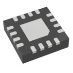 CDCLVP2102RGTT

The activity of extra discounts on wholesale prices is in full swing…
Please fill in your contact information and we will send you the latest wholesale price list.





