 ChipApex | Global Electronic Components Supplier

SEARCH
Search Product
Search Post
— IC芯片 | 连接器 | 传感器 | 被动器件 —
Search productSearch post
— IC芯片 | 连接器 | 传感器 | 被动器件 —
Consult the customer manager about the wholesale price.
consultation hotline:86-132-6715-2157
email:[email protected]
Contact the product manager for consultation. One-stop consultation is available.
Do you want a lower wholesale price? Please send us your inquiry and we will reply immediately.
The CDCS504TPWRQ1 is an automotive-grade clock multiplier and buffer manufactured by Texas Instruments. It features a single circuit with a 1:1 input-to-output ratio, utilizing LVCMOS logic for both input and output signals. The device supports a maximum operating frequency of 108 MHz and operates within a supply voltage range of 3 V to 3.6 V. It is housed in an 8-TSSOP package (0.173 inch width) designed for surface-mount installation. The component meets AEC-Q100 qualification standards and functions reliably across an extended temperature range from -40°C to +105°C.
Verify the specific ordering suffix against the manufacturer's official documentation to confirm package type and reel specifications. Ensure that the selected variant matches the required automotive grade and temperature rating for the intended application environment. Cross-reference the datasheet for any recent design changes or pin configuration updates before finalizing procurement orders.
Select this component when a 1:1 clock multiplication function is required for automotive applications. Confirm that the system power supply remains within the 3 V to 3.6 V range to ensure proper operation. Verify that the LVCMOS signal compatibility aligns with the connected source and load devices. Ensure the PCB layout accommodates the 8-TSSOP footprint dimensions for correct assembly.
This part belongs to the CDCS50x family of clock multipliers and buffers from Texas Instruments. The 'Q1' suffix indicates automotive qualification under AEC-Q100 standards. The 'T' suffix typically denotes tape and reel packaging. This series provides low-power solutions for distributing and multiplying clock signals in demanding electronic systems.
Consult the official TI replacement matrix for verified cross-references. Ensure any substitute component maintains the same 1:1 ratio, LVCMOS I/O levels, and AEC-Q100 automotive qualification. Verify package compatibility and electrical parameter alignment before implementation.
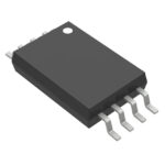 CDCS504TPWRQ1

The activity of extra discounts on wholesale prices is in full swing…
Please fill in your contact information and we will send you the latest wholesale price list.




