 ChipApex | Global Electronic Components Supplier
SEARCH
Search Product
Search Post
— IC芯片 | 连接器 | 传感器 | 被动器件 —
Search productSearch post
— IC芯片 | 连接器 | 传感器 | 被动器件 —
Consult the customer manager about the wholesale price.
consultation hotline:86-132-6715-2157
email:[email protected]
Contact the product manager for consultation. One-stop consultation is available.
Do you want a lower wholesale price? Please send us your inquiry and we will reply immediately.
The CSD23201W10 is a P-channel NexFET Power MOSFET designed for ultra-low resistance and gate charge in a compact footprint. It features a –12 V drain-to-source voltage rating and a continuous drain current of –2.2 A at 25°C case temperature. The device offers an on-resistance (RDS(on)) as low as 66 mΩ at VGS = –4.5V. Key dynamic parameters include a total gate charge (Qg) of 1.8 nC and a gate-to-drain charge (Qgd) of 0.26 nC. It operates within a junction temperature range of –55°C to +150°C and utilizes a 1mm × 1mm wafer-level CSP package.
Verify the specific ordering suffix and media quantity against the manufacturer's official documentation before procurement. Confirm that the component meets RoHS compliance requirements for your target market. Ensure that handling procedures account for the limited built-in ESD protection by using conductive foam or shorting leads during storage and assembly to prevent electrostatic damage to the MOS gates.
Select this component when minimizing board space is critical due to its 1mm x 1mm wafer-level package. It is suitable for applications requiring fast switching speeds, indicated by low Qg and Qgd values. Consider the thermal resistance characteristics and maximum power dissipation limits relative to your PCB copper area. Verify that the required gate drive voltage aligns with the specified RDS(on) performance curves for optimal efficiency.
This part belongs to Texas Instruments' NexFET family of power MOSFETs, which are engineered to deliver low on-resistance and gate charge. The CSD23201W10 specifically targets portable and battery-powered devices where size constraints and power efficiency are paramount. It serves as a single-channel solution for managing power flow in compact electronic designs.
Consult the manufacturer's product folder for officially confirmed substitute part numbers. Do not assume functional equivalence based solely on similar electrical ratings without verifying pinout compatibility and package dimensions.
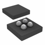 CSD23201W10
The activity of extra discounts on wholesale prices is in full swing…
Please fill in your contact information and we will send you the latest wholesale price list.





