 ChipApex | Global Electronic Components Supplier
SEARCH
Search Product
Search Post
— IC芯片 | 连接器 | 传感器 | 被动器件 —
Search productSearch post
— IC芯片 | 连接器 | 传感器 | 被动器件 —
Consult the customer manager about the wholesale price.
consultation hotline:86-132-6715-2157
email:[email protected]
Contact the product manager for consultation. One-stop consultation is available.
Do you want a lower wholesale price? Please send us your inquiry and we will reply immediately.
The CSD25201W15 is a P-Channel NexFET Power MOSFET designed for battery-operated, space-constrained applications. It features a wafer level package with dimensions of 1.5 mm x 1.5 mm. Key electrical parameters include a drain-to-source voltage (BVDSS) of -20 V and a continuous drain current (ID) of 4 A. The device offers low on-state resistance (RDS(on)) ranging from 33 mΩ to 52 mΩ depending on gate drive conditions. Total gate charge (Qg) is specified at 4.3 nC typical. Thermal performance includes a junction-to-ambient thermal resistance (RθJA) of 185 °C/W on a minimum copper footprint.
Verify component authenticity by checking the manufacturer's marking code against official datasheet specifications. Confirm the package type matches the required wafer level form factor. Ensure the ordering suffix corresponds to the correct media quantity and reel configuration. Cross-reference the RoHS compliance status with current environmental regulations before finalizing procurement orders.
Select this component when minimizing board area is critical due to its ultra-small outline. Evaluate the RDS(on) values against the specific gate drive voltage available in the system to ensure adequate current handling. Consider the thermal resistance requirements based on the expected copper footprint area. Verify that the -20 V rating aligns with the maximum operating voltage of the target application.
This device belongs to Texas Instruments' NexFET Power MOSFET family, which focuses on delivering high performance in compact packages. The CSD25201W15 utilizes silicon technology optimized for low resistance and fast switching speeds. It is part of a series designed specifically for portable electronics and battery-powered devices where size and efficiency are paramount constraints.
Consult the manufacturer's datasheet for similar part numbers within the same NexFET series. Verify pinout compatibility and electrical parameter equivalence before substitution. Ensure any replacement maintains the required wafer level package dimensions and thermal characteristics.
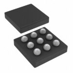 CSD25201W15
The activity of extra discounts on wholesale prices is in full swing…
Please fill in your contact information and we will send you the latest wholesale price list.





