 ChipApex | Global Electronic Components Supplier
SEARCH
Search Product
Search Post
— IC芯片 | 连接器 | 传感器 | 被动器件 —
Search productSearch post
— IC芯片 | 连接器 | 传感器 | 被动器件 —
Consult the customer manager about the wholesale price.
consultation hotline:86-132-6715-2157
email:[email protected]
Contact the product manager for consultation. One-stop consultation is available.
Do you want a lower wholesale price? Please send us your inquiry and we will reply immediately.
The CTS100EL16VOTG is an LVPECL oscillator gain stage and buffer with enable, housed in an MSOP8 package. It provides differential outputs (Q/Q¯) and high-gain outputs (QHG/Q¯HG). The device operates on a single supply voltage ranging from +3.0 V to +5.5 V or dual supplies of -3.0 V to -5.5 V. Key electrical parameters include a typical propagation delay of 250 ps, a power supply current of 40 mA, and a bandwidth exceeding 1 GHz. The component supports ECL/PECL input signals and features an internal 75 kΩ pull-down resistor on the enable pin.
Verify the specific ordering suffix to confirm the package type, as the base part number covers multiple variants including MLP8 and MSOP10. Ensure the selected variant matches the required footprint and pinout configuration for the target PCB layout. Cross-reference the datasheet revision date to confirm the accuracy of the electrical specifications before finalizing procurement orders.
Select this component when a high-bandwidth buffer with independent control over high-gain outputs is required. Verify that the system logic levels are compatible with the specified ECL or CMOS input ranges. Confirm that the thermal environment remains within the -40 °C to +85 °C operating range to maintain the guaranteed propagation delay and noise floor specifications.
This component belongs to the CTS100EL16 family of LVPECL buffers manufactured by CTS Corporation. The family includes variants such as the CTS100EL16VONG in an MLP8 package and the CTS100EL16VOUG in an MSOP10 package. All variants share identical core functionality but differ in physical dimensions and pin assignments.
Direct substitutes are not explicitly listed in the official documentation. Designers should evaluate other LVPECL buffers from CTS or competitors based on matching propagation delay, supply voltage compatibility, and package footprint constraints.
When the EN¯¯ pin is driven HIGH, the QHG/Q¯HG outputs are forced to LOW/HIGH states respectively. When EN¯¯ is LOW or floating, the input data is passed through to these outputs normally.
Outputs should be terminated via 50 Ω resistors to VCC - 2 V or using a Thevenin equivalent network. Unused outputs may be left floating.
Yes, the EN¯¯ input can be driven by CMOS logic signals. For the D/D¯ inputs, AC coupling with appropriate series resistors (e.g., 430 Ω for 3.3 V CMOS) is recommended to achieve the correct input swing.
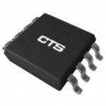 CTS100EL16VOTG
The activity of extra discounts on wholesale prices is in full swing…
Please fill in your contact information and we will send you the latest wholesale price list.





