 ChipApex | Global Electronic Components Supplier

SEARCH
Search Product
Search Post
— IC芯片 | 连接器 | 传感器 | 被动器件 —
Search productSearch post
— IC芯片 | 连接器 | 传感器 | 被动器件 —
Consult the customer manager about the wholesale price.
consultation hotline:86-132-6715-2157
email:[email protected]
Contact the product manager for consultation. One-stop consultation is available.
Do you want a lower wholesale price? Please send us your inquiry and we will reply immediately.
CTSLV315QG is listed in the Clock Buffers, Drivers range at ChipApex. The manufacturer field lists CTS-Frequency Controls. Its product description is IC CLK BUFFER 1:2 1.6GHZ 8SON. Review the specifications below when checking this part for your BOM.
The CTSLV315 is a configurable ultra-low phase noise LVPECL and LVDS buffer and translator IC designed for high-performance clock distribution. It operates on a 2.375V to 3.6V supply and supports input frequencies up to 1GHz in ÷1 mode or 1.6GHz in ÷2 mode. The device provides selectable output formats (LVPECL or LVDS), division ratios, and enable polarity via static configuration bits. Key electrical specifications include a phase noise floor of -167dBc/Hz for LVPECL and -165dBc/Hz for LVDS at 1MHz offset. Integrated jitter is specified at 26fs for LVPECL and 36fs for LVDS over a 12kHz-20MHz bandwidth.
Verify the specific package variant required for the application, as the CTSLV315 is available in both SON8 (suffix QG) and MSOP8 (suffix TG). Confirm that the selected configuration bits align with the desired output format and enable polarity before finalizing the order. Ensure the design accommodates the necessary termination resistors for the chosen output standard.
Select the CTSLV315 when an ultra-low phase noise buffer is needed for signals below 0.6 Vp-p. For higher signal levels without gain requirements, consider the CTSLV310. Designers must configure the b-0 and b-1 pins to set the output type and division ratio. Ensure the input signal swing is at least 750mVpp to meet AC specifications and use AC coupling to maintain duty cycle integrity.
The CTSLV315 belongs to CTS-Frequency Controls' family of low-noise clock buffers. It serves as a flexible solution for translating oscillator signals into differential formats. The device distinguishes itself through its configurable nature, allowing a single component to replace multiple fixed-function buffers by adjusting static pin states.
For applications with higher signal levels that do not require gain, the CTSLV310 is recommended as an alternative. Verify compatibility regarding supply voltage ranges and output drive capabilities when substituting.
Explore related parts through Clock/Timing, Integrated Circuits (ICs), all product categories, ChipApex homepage.
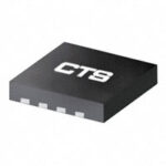 CTSLV315QG

The activity of extra discounts on wholesale prices is in full swing…
Please fill in your contact information and we will send you the latest wholesale price list.





