 ChipApex | Global Electronic Components Supplier

SEARCH
Search Product
Search Post
— IC芯片 | 连接器 | 传感器 | 被动器件 —
Search productSearch post
— IC芯片 | 连接器 | 传感器 | 被动器件 —
Consult the customer manager about the wholesale price.
consultation hotline:86-132-6715-2157
email:[email protected]
Contact the product manager for consultation. One-stop consultation is available.
Do you want a lower wholesale price? Please send us your inquiry and we will reply immediately.
CTSLV353QG is listed in the Clock Buffers, Drivers range at ChipApex. The manufacturer field lists CTS-Frequency Controls. Its product description is IC CLK BUFFER 1:1 800MHZ 8QFN. Review the specifications below when checking this part for your BOM.
The CTSLV353 is a sine wave/CMOS to LVPECL buffer and translator optimized for very low phase noise (-165dBc/Hz). It converts crystal or SAW-based oscillators into LVPECL outputs with up to 800MHz bandwidth. The device features selectable ÷1 or ÷2 output division ratios and configurable enable logic (active high or low). It operates on a single 3.0V to 3.6V supply, drawing a typical current of 35mA. The component is housed in an 8-QFN (1.5x1.5mm) surface-mount package and supports an operating temperature range of -40°C to +85°C.
Verify the specific package variant required for the design; the QG suffix denotes the 8-QFN package while PG denotes SON8. Confirm that the application circuit provides proper AC coupling and termination resistors to meet AC specifications. Ensure the power supply voltage remains within the 3.0V to 3.6V range during operation.
Select the CTSLV353 when LVPECL outputs are required from CMOS or sine wave inputs with bandwidths up to 800MHz. Choose this part over the CTSLV363 if lower cost or specific ÷1/÷2 selection logic is preferred, noting the CTSLV363 offers higher bandwidth (≥1GHz). Verify that the 1.5x1.5mm QFN footprint fits the PCB layout constraints.
The CTSLV353 belongs to the CTSLV35x family of buffers and translators. It shares functional similarities with the CTSLV351 (fixed ÷1) and CTSLV363 (higher bandwidth), offering designers flexibility in division ratio and enable logic configuration within the same low-phase-noise architecture.
Public confirmed substitute part numbers are not available in the provided documentation.
The divide ratio is selected using the DIV_SEL pin. A Low or NC state configures the device for ÷1 mode, while a High state configures it for ÷2 mode.
For clock applications, an input signal of at least 750mVPP ensures the device meets AC specifications. The maximum recommended input signal is VDD VPP.
Outputs should be terminated identically to avoid waveform distortion. Standard termination uses two 50Ω resistors connected between the outputs and VDD-2.0V.
Explore related parts through Clock/Timing, Integrated Circuits (ICs), all product categories, ChipApex homepage.
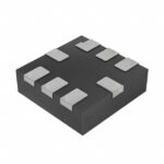 CTSLV353QG

The activity of extra discounts on wholesale prices is in full swing…
Please fill in your contact information and we will send you the latest wholesale price list.





