 ChipApex | Global Electronic Components Supplier
SEARCH
Search Product
Search Post
— IC芯片 | 连接器 | 传感器 | 被动器件 —
Search productSearch post
— IC芯片 | 连接器 | 传感器 | 被动器件 —
Consult the customer manager about the wholesale price.
consultation hotline:86-132-6715-2157
email:[email protected]
Contact the product manager for consultation. One-stop consultation is available.
Do you want a lower wholesale price? Please send us your inquiry and we will reply immediately.
The CTSLV399TG is an LVPECL/LVDS oscillator gain stage and buffer with selectable enable, manufactured by CTS-Frequency Controls. It operates on a 3V to 5.5V power supply within a -40°C to +85°C temperature range. The device features a single-ended data input (D) and provides both PECL outputs (Q/Q¯) and LVDS outputs (QHG/Q¯HG). Key electrical parameters include a propagation delay of 400 ps for the Q output and 550 ps for the LVDS output. The MSOP8 package version supports CMOS/TTL level enable inputs.
Verify the specific ordering suffix 'T' confirms the MSOP8 package configuration. Ensure the design accounts for the 'Not recommended for new designs' status indicated in the documentation. Confirm that the selected enable pin configuration matches the required logic threshold for the system environment.
Select this component when an LVDS output buffer is required alongside a PECL output from a single input source. The MSOP8 package is suitable for space-constrained applications. Verify that the input swing requirements fall within the specified ±80 mV to ±1000 mV range for proper AC coupling operation.
The CTSLV399TG belongs to the CTSLV399 family of specialized oscillator gain stages. It serves as a bridge between high-speed oscillators and downstream logic, offering dual-output capability. The TG suffix specifically denotes the MSOP8 surface-mount package variant, distinguishing it from the MLP8 package options available in the same series.
The datasheet notes similar operation to the CTS100LVEL16VT, though the latter utilizes different output characteristics. No direct public substitute part numbers are documented for the CTSLV399TG.
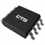 CTSLV399TG
The activity of extra discounts on wholesale prices is in full swing…
Please fill in your contact information and we will send you the latest wholesale price list.




