 ChipApex | Global Electronic Components Supplier

SEARCH
Search Product
Search Post
— IC芯片 | 连接器 | 传感器 | 被动器件 —
Search productSearch post
— IC芯片 | 连接器 | 传感器 | 被动器件 —
Consult the customer manager about the wholesale price.
consultation hotline:86-132-6715-2157
email:[email protected]
Contact the product manager for consultation. One-stop consultation is available.
Do you want a lower wholesale price? Please send us your inquiry and we will reply immediately.
CY2308SXI-1 is listed in the Clock Generators, PLLs, Frequency Synthesizers range at ChipApex. The manufacturer field lists Infineon Technologies. Its product description is IC FANOUT BUFFER 16SOIC. Review the specifications below when checking this part for your BOM.
The CY2308SXI-1 is a 3.3 V Zero Delay Buffer manufactured by Infineon Technologies, designed for distributing high-speed clocks in PC, workstation, datacom, and telecom applications. It features an on-chip PLL that locks to an input clock presented on the REF pin, with feedback driven from an external FBK pin connected to one of eight outputs. The device operates within a frequency range of 10 MHz to 133 MHz and supports two banks of four three-stateable outputs. Key electrical parameters include a supply voltage (VDD) range of 3.0 V to 3.6 V, typical cycle-to-cycle jitter of 75 ps at 66 MHz with a 15 pF load, and input-to-output skew less than 250 ps. It is available in a 16-pin SOIC package and supports industrial temperature operation from -40 °C to +85 °C.
Verify component authenticity through authorized distributors or direct manufacturer channels. Confirm RoHS compliance status and check for end-of-life notifications, as this part may be subject to obsolescence. Ensure proper handling for moisture sensitivity levels during storage and assembly processes.
Select the CY2308SXI-1 when zero-delay buffering is required for 3.3 V systems operating up to 133 MHz. Consider the -1H variant if faster rise and fall times are necessary. Verify that the application requires industrial temperature range (-40 °C to +85 °C) and ensure adequate load capacitance management for skew control.
The CY2308 series includes variants such as CY2308-1, -1H, -2, -3, -4, and -5H, offering different frequency multiplication options and drive strengths. The -1 variant provides reference frequency outputs, while the -1H offers higher drive capability. Other variants enable 2x or 4x frequency multiplication depending on the feedback path configuration.
Direct substitutes include other CY2308 family members like CY2308SXI-1H for enhanced drive strength. Cross-family replacements require verification of voltage levels, package compatibility, and jitter specifications.
Zero delay is achieved by connecting one of the outputs to the FBK pin and ensuring all outputs, including the feedback output, have equal capacitive loading.
The PLL enters a power-down state, three-stating all outputs and turning off the PLL, resulting in current draw of less than 25 µA.
Yes, multiple devices can accept the same input clock, with device-to-device skew specified as less than 700 ps.
Explore related parts through Clock/Timing, Integrated Circuits (ICs), all product categories, ChipApex homepage.
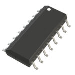 CY2308SXI-1

The activity of extra discounts on wholesale prices is in full swing…
Please fill in your contact information and we will send you the latest wholesale price list.





