 ChipApex | Global Electronic Components Supplier

SEARCH
Search Product
Search Post
— IC芯片 | 连接器 | 传感器 | 被动器件 —
Search productSearch post
— IC芯片 | 连接器 | 传感器 | 被动器件 —
Consult the customer manager about the wholesale price.
consultation hotline:86-132-6715-2157
email:[email protected]
Contact the product manager for consultation. One-stop consultation is available.
Do you want a lower wholesale price? Please send us your inquiry and we will reply immediately.
CY23S05SXC-1 is listed in the Clock Generators, PLLs, Frequency Synthesizers range at ChipApex. The manufacturer field lists Cypress Semiconductor Corp. Its product description is PLL BASED CLOCK DRIVER, 23S SERI. Review the specifications below when checking this part for your BOM.
The CY23S05SXC-1 is a low-cost, 3.3 V spread-aware zero delay buffer manufactured by Cypress Semiconductor. It accepts one reference input and drives five low-skew outputs using an on-chip phase-locked loop (PLL). The device operates within a frequency range of 10 MHz to 100 MHz and supports up to 133.33 MHz. Key electrical parameters include an output-to-output skew of less than 250 ps, a cycle-to-cycle jitter of under 200 ps, and an input-to-output propagation delay of 0 ± 350 ps. It utilizes advanced 0.65 µm CMOS technology and is housed in an 8-pin, 150-mil SOIC package.
Verify the specific ordering suffix for package type and temperature range. The 'C' suffix indicates Commercial temperature (0°C to 70°C), while 'I' denotes Industrial (-40°C to 85°C). The 'X' indicates a lead-free SOIC package. Confirm whether standard drive ('1') or high drive ('1H') is required, as rise/fall times differ significantly between these variants. Check for tape and reel availability if automated assembly is needed.
Select the CY23S05SXC-1 for applications requiring exactly five buffered clock outputs from a single reference source. Ensure all outputs, including CLKOUT, are loaded equally to achieve zero input-output delay; use the datasheet graph to calculate loading differences if delay adjustment is necessary. For frequencies above 100 MHz, limit load capacitance to 10 pF, whereas 30 pF is permissible below 100 MHz. Choose the -1H variant if faster rise and fall times are critical for signal integrity.
The CY23S05SXC-1 is the 5-output version of the CY23S09 series. While the CY23S09 provides nine outputs grouped into two banks of four plus one, the CY23S05 simplifies the design for lower fan-out requirements. Both devices share identical PLL architecture, operating voltages, and package options, allowing for design flexibility based on output count needs.
Direct functional replacements within the same family include the CY23S09SXC-1 for higher output counts. For legacy leaded packages, the CY23S05SC-1 was the equivalent part before the transition to lead-free SX suffixes. Verify that any substitute maintains the 3.3 V supply requirement and 0.65 µm CMOS process characteristics to ensure compatibility with existing PCB layouts and power supplies.
Zero delay is obtained by ensuring all outputs, including the CLKOUT pin used for internal PLL feedback, have equal capacitive loads. Adjusting the load difference between CLKOUT and other outputs allows for precise delay tuning.
The maximum load capacitance is 30 pF for operating frequencies below 100 MHz. For frequencies ranging from 100 MHz to 133.33 MHz, the load capacitance must be limited to 10 pF.
Yes, the CY23S05SXC-1 is Spread Aware and does not filter out Spread Spectrum features from the reference input, preventing tracking skew issues in synchronized systems.
Explore related parts through Clock/Timing, Integrated Circuits (ICs), all product categories, ChipApex homepage.
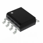 CY23S05SXC-1

The activity of extra discounts on wholesale prices is in full swing…
Please fill in your contact information and we will send you the latest wholesale price list.





