 ChipApex | Global Electronic Components Supplier

SEARCH
Search Product
Search Post
— IC芯片 | 连接器 | 传感器 | 被动器件 —
Search productSearch post
— IC芯片 | 连接器 | 传感器 | 被动器件 —
Consult the customer manager about the wholesale price.
consultation hotline:86-132-6715-2157
email:[email protected]
Contact the product manager for consultation. One-stop consultation is available.
Do you want a lower wholesale price? Please send us your inquiry and we will reply immediately.
CY28317PVXC-2 is listed in the Application Specific Clock/Timing range at ChipApex. The manufacturer field lists Skyworks Solutions Inc.. Its product description is IC CLK FTG VIA PL/E133T 48SSOP. Review the specifications below when checking this part for your BOM.
The CY28317PVXC-2 is a single-chip system frequency synthesizer designed for mobile VIA PL133T and PLE133T chipsets. It generates programmable CPU, PCI, and SDRAM clock outputs with less than 1 MHz increment resolution. The device integrates an SMBus interface for configuration, a fail-safe Watchdog Timer for system recovery, and Spread Spectrum technology to maximize EMI suppression. Key electrical specifications include a CPU-to-CPU output skew of 175 ps and a PCI-to-PCI output skew of 500 ps. It operates with 3.3V supplies for core logic and 2.5V for CPU outputs, housed in a 48-pin SSOP or TSSOP package.
Verify the component matches the exact part number CY28317PVXC-2. Confirm the package type is either 48-pin SSOP or TSSOP as specified. Ensure the device is from a recognized manufacturer such as Cypress Semiconductor or Silabs, as indicated in the documentation. Check for any specific revision markings that might affect compatibility with the target motherboard design.
Select this component when designing systems based on VIA PL133T or PLE133T chipsets requiring precise clock synchronization. Consider the programmable output skew features if tight timing margins are necessary between CPU, PCI, and SDRAM clocks. The integrated Watchdog Timer and automatic recovery mechanisms make it suitable for applications requiring high system reliability and fault tolerance.
The CY28317 series is part of a family of clock generators developed by Cypress Semiconductor, now part of Silicon Labs. These devices are specifically tailored for mobile computing platforms, providing the necessary clock signals for processors, memory, and peripheral interfaces. The CY28317PVXC-2 variant offers enhanced features like programmable drive strength and detailed skew control to meet the stringent requirements of modern mobile architectures.
Direct replacements may include other CY28317 variants with different package options or speed grades. Verify pin compatibility and register settings when substituting. Cross-reference with similar clock generators from other manufacturers only if functional equivalence can be confirmed through detailed datasheet comparison.
The CY28317PVXC-2 supports programmable CPU frequencies ranging from 50 MHz to 248 MHz.
The Watchdog Timer monitors system stability. If a time-out occurs, it generates a system reset and switches the clock outputs to a pre-configured recovery frequency to restore system operation.
Yes, the drive strength for SDRAM, PCI, and CPU outputs can be programmed via the SMBus interface to optimize signal integrity and power consumption.
Explore related parts through Clock/Timing, Integrated Circuits (ICs), all product categories, ChipApex homepage.
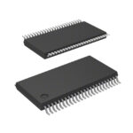 CY28317PVXC-2

The activity of extra discounts on wholesale prices is in full swing…
Please fill in your contact information and we will send you the latest wholesale price list.





