 ChipApex | Global Electronic Components Supplier

SEARCH
Search Product
Search Post
— IC芯片 | 连接器 | 传感器 | 被动器件 —
Search productSearch post
— IC芯片 | 连接器 | 传感器 | 被动器件 —
Consult the customer manager about the wholesale price.
consultation hotline:86-132-6715-2157
email:[email protected]
Contact the product manager for consultation. One-stop consultation is available.
Do you want a lower wholesale price? Please send us your inquiry and we will reply immediately.
CY28341OC-2 is listed in the Application Specific Clock/Timing range at ChipApex. The manufacturer field lists Cypress Semiconductor Corp. Its product description is FTG FOR VIA P4 CHIPSET. Review the specifications below when checking this part for your BOM.
The CY28341OC-2 is a PLL-based clock generator designed for VIA P4 chipset systems supporting DDR applications. It features two independent circuits with a 1:20 input-to-output ratio, distributing a crystal input to twenty differential clock outputs. The device operates at a maximum frequency of 200 MHz and supports dual voltage supplies of 2.375 V and 3.135 V. Packaged in a 56-pin SSOP, it functions within an ambient temperature range of 0°C to 70°C.
Verify the specific ordering suffix against official Cypress documentation to confirm package type and temperature grade. Ensure the required supply voltages match the design specifications. Confirm RoHS compliance status as historical data may vary by production batch.
Select this component when designing for VIA P4 architectures requiring synchronized DDR clock distribution. Ensure the PCB layout accommodates the 56-SSOP footprint. Verify that the system power rails provide stable 2.375 V and 3.135 V supplies for proper PLL operation.
This part belongs to the CY28341 family of universal single-chip clock solutions. It is specifically optimized for VIA P4M/KT/KM400 series chipsets. The device integrates multiple clock generators to reduce board space compared to discrete timing components.
Check for CY28341 variants with different suffixes for package or temperature differences. Consult Skyworks Solutions documentation for direct pin-compatible replacements if Cypress inventory is unavailable.
Explore related parts through Clock/Timing, Integrated Circuits (ICs), all product categories, ChipApex homepage.
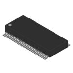 CY28341OC-2

The activity of extra discounts on wholesale prices is in full swing…
Please fill in your contact information and we will send you the latest wholesale price list.





