 ChipApex | Global Electronic Components Supplier

SEARCH
Search Product
Search Post
— IC芯片 | 连接器 | 传感器 | 被动器件 —
Search productSearch post
— IC芯片 | 连接器 | 传感器 | 被动器件 —
Consult the customer manager about the wholesale price.
consultation hotline:86-132-6715-2157
email:[email protected]
Contact the product manager for consultation. One-stop consultation is available.
Do you want a lower wholesale price? Please send us your inquiry and we will reply immediately.
CY29948AC is listed in the Clock Buffers, Drivers range at ChipApex. The manufacturer field lists Cypress Semiconductor Corp. Its product description is IC CLK BUFFER 2:12 200MHZ 32TQFP. Review the specifications below when checking this part for your BOM.
The CY29948AC is a low-voltage clock distribution buffer supporting 2.5 V or 3.3 V operation with a maximum frequency of 200 MHz. It features a 1:12 output ratio, accepting either differential LVPECL or single-ended LVCMOS/LVTTL inputs. The device provides 12 LVCMOS/LVTTL-compatible outputs capable of driving up to 24 transmission lines in series-terminated configurations. Key electrical parameters include a typical output-to-output skew of 150 ps and propagation delays ranging from 4.0 ns to 10.9 ns depending on voltage and input source. It operates within a commercial temperature range of 0°C to +70°C.
Verify the specific suffix 'AC' against official ordering codes. Datasheet lists CY29948AXC for Commercial (0°C to +70°C) and CY29948AXI for Industrial (-40°C to +85°C). Confirm if 'AC' denotes a specific package variant or legacy designation not explicitly detailed in the current Rev *J document.
Select this component when a 1:12 fanout buffer is required for high-speed synchronous designs. Ensure the input signal matches the supported LVPECL or LVCMOS/LVTTL standards. Verify that the thermal resistance of 65 °C/W is acceptable for the application's ambient conditions without additional heatsinking.
The CY29948 belongs to Cypress Semiconductor's family of low-voltage clock buffers. It is pin-compatible with MPC948, MPC948L, and MPC9448 devices, facilitating direct replacements in existing designs requiring similar clock distribution capabilities.
Pin-compatible substitutes include MPC948, MPC948L, and MPC9448. Verify voltage levels and temperature ranges match the original design requirements before substitution.
The device uses a synchronous output enable input (SYNC_OE) that is internally synchronized to the input clock. This synchronization eliminates potential output glitching or runt pulse generation.
Each output can drive one or two traces, providing an effective fanout of 1:24 for the entire device when using series terminated transmission lines.
No, the outputs are controlled collectively via the SYNC_OE pin for enabling/disabling and the TS# pin for three-stating. All outputs respond simultaneously to these control signals.
Explore related parts through Clock/Timing, Integrated Circuits (ICs), all product categories, ChipApex homepage.
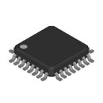 CY29948AC

The activity of extra discounts on wholesale prices is in full swing…
Please fill in your contact information and we will send you the latest wholesale price list.






