 ChipApex | Global Electronic Components Supplier
SEARCH
Search Product
Search Post
— IC芯片 | 连接器 | 传感器 | 被动器件 —
Search productSearch post
— IC芯片 | 连接器 | 传感器 | 被动器件 —
Consult the customer manager about the wholesale price.
consultation hotline:86-132-6715-2157
email:[email protected]
Contact the product manager for consultation. One-stop consultation is available.
Do you want a lower wholesale price? Please send us your inquiry and we will reply immediately.
The CY2DL814ZXC is a 1:4 clock fanout buffer from the ComLink™ series, manufactured by Cypress Semiconductor Corp. It operates on a single 3.3V supply (3.135V to 3.465V) and supports a maximum frequency of 400 MHz. The device features a configurable input compatible with LVDS, LVPECL, or LVTTL signals, driving four differential LVDS output pairs. Key electrical parameters include a typical propagation delay of 4 ns and an output-to-output skew of 85 ps. It is housed in a 16-TSSOP package and rated for commercial operating temperatures between 0°C and 70°C.
Verify the specific suffix 'ZXC' confirms the commercial temperature range (0°C to 70°C) and TSSOP package type as listed in the ordering information. Ensure the source document matches the revision *B datasheet for accurate pin definitions and electrical characteristics. Confirm lead-free status if required by assembly specifications.
Select this component when a low-voltage 3.3V fanout buffer is required for LVDS distribution. The CY2DL814 allows input flexibility across LVDS, LVPECL, and LVTTL standards via the CONFIG pin. Consider the 85 ps skew specification for tight timing requirements and verify that the 400 MHz maximum frequency meets the system clock speed needs.
The CY2DL814 belongs to the ComLink™ series of network circuits produced using 0.35-micron CMOS technology. This series focuses on high-speed logic applications, providing industry-fast signal buffering. The part number CY2DL814ZXC specifically denotes the commercial grade variant in a 16-pin TSSOP package.
Public confirmed substitute part numbers are not available in the provided documentation. Check for other members of the ComLink™ series such as the CY2DP814 or CY2PD817 for different fanout ratios or input/output configurations.
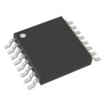 CY2DL814ZXC
The activity of extra discounts on wholesale prices is in full swing…
Please fill in your contact information and we will send you the latest wholesale price list.





