 ChipApex | Global Electronic Components Supplier
SEARCH
Search Product
Search Post
— IC芯片 | 连接器 | 传感器 | 被动器件 —
Search productSearch post
— IC芯片 | 连接器 | 传感器 | 被动器件 —
Consult the customer manager about the wholesale price.
consultation hotline:86-132-6715-2157
email:[email protected]
Contact the product manager for consultation. One-stop consultation is available.
Do you want a lower wholesale price? Please send us your inquiry and we will reply immediately.
The CY2DL814ZXI is a 1:4 clock fanout buffer from the ComLink™ series, manufactured by Cypress Semiconductor Corp. It operates on a single 3.3V supply (3.135V to 3.465V) and supports maximum frequencies of 400 MHz with a 50% duty cycle or 200 MHz with a 20% duty cycle. The device features a configurable differential input compatible with LVDS, LVPECL, or LVTTL/LVCMOS logic levels. It provides four differential LVDS output pairs with selectable standard or high drive capabilities for 50-ohm or 100-ohm loads. Typical propagation delay is 4 ns, and output-to-output skew is 85 ps. It is housed in a 16-TSSOP package and rated for industrial temperatures (-40°C to +85°C).
Verify the ordering suffix 'XI' confirms the lead-free industrial grade specification (-40°C to +85°C) and TSSOP package type. Confirm that the specific revision matches the required datasheet version for AC parameter accuracy. Ensure the supplier source provides the original manufacturer documentation rather than third-party interpretations.
Select this component when a low-skew distribution of LVDS clocks is required from various input standards. The CNTRL pin allows adjustment of output drive strength for different line impedances. Verify that the input signal amplitude meets the minimum requirements for the chosen configuration mode (LVDS vs. LVPECL vs. LVTTL).
This part belongs to the ComLink™ series of network circuits produced using 0.35-micron CMOS technology. The CY2DL814 variant specifically addresses the need for buffering and translating clock signals in high-speed data communication systems. It reduces loading on the source clock while providing multiple clean output phases.
The CY2DL814ZI is the non-lead-free equivalent of the CY2DL814ZXI. Both share identical electrical characteristics and pinouts but differ in environmental compliance specifications.
The drive strength is controlled by the CNTRL pin (Pin 3). A logic low selects standard drive (defaulting to 100-ohm), while a logic high selects high drive/bus mode (defaulting to 50-ohm).
The device supports up to 400 MHz with a 50% duty cycle and up to 200 MHz with a 20% duty cycle.
Yes, the input can be configured for LVTTL or LVCMOS single-ended signals by setting the CONFIG pin (Pin 2) to a logic high.
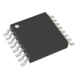 CY2DL814ZXI
The activity of extra discounts on wholesale prices is in full swing…
Please fill in your contact information and we will send you the latest wholesale price list.






