 ChipApex | Global Electronic Components Supplier
SEARCH
Search Product
Search Post
— IC芯片 | 连接器 | 传感器 | 被动器件 —
Search productSearch post
— IC芯片 | 连接器 | 传感器 | 被动器件 —
Consult the customer manager about the wholesale price.
consultation hotline:86-132-6715-2157
email:[email protected]
Contact the product manager for consultation. One-stop consultation is available.
Do you want a lower wholesale price? Please send us your inquiry and we will reply immediately.
The CY2DP1502SXI is a 1:2 fanout clock buffer manufactured by Infineon Technologies, designed for high-frequency signal distribution. It supports input formats including CML, HCSL, LVDS, and LVPECL, while providing differential LVPECL outputs. The device operates within a supply voltage range of 2.375V to 3.465V and supports frequencies up to 1.5 GHz. Packaged in an 8-SOIC surface-mount case with a width of 3.90mm, it functions reliably across an operating temperature range of -40°C to 85°C.
This component is identified as End-of-Life (EOL) by the manufacturer. Current availability is limited to existing stock, with quantities restricted by minimum order requirements for volumes exceeding immediate inventory. Verification of current lifecycle status and substitute options is recommended before finalizing procurement plans due to discontinuation.
Select this buffer when a single clock source must be distributed to two differential LVPECL loads. Ensure the system power supply remains between 2.375V and 3.465V. Verify that the input signal conforms to one of the supported standards (CML, HCSL, LVDS, or LVPECL). Consider the 8-SOIC package constraints for PCB layout and thermal management within the -40°C to 85°C operational range.
The CY2DP1502SXI belongs to the CY2Dx series of non-PLL fanout buffers from Infineon. These devices are engineered to provide low-jitter clock distribution without the complexity of phase-locked loops. They are often used in conjunction with other clock generators to form complete high-frequency clock tree solutions, offering industry-leading added jitter performance typical of the series.
As the CY2DP1502SXI is discontinued, engineers should evaluate alternative 1:2 fanout buffers from the same family or compatible competitors. Verify pin compatibility and electrical specifications such as supply voltage and output swing when selecting a direct replacement.
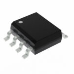 CY2DP1502SXI
The activity of extra discounts on wholesale prices is in full swing…
Please fill in your contact information and we will send you the latest wholesale price list.




