 ChipApex | Global Electronic Components Supplier
SEARCH
Search Product
Search Post
— IC芯片 | 连接器 | 传感器 | 被动器件 —
Search productSearch post
— IC芯片 | 连接器 | 传感器 | 被动器件 —
Consult the customer manager about the wholesale price.
consultation hotline:86-132-6715-2157
email:[email protected]
Contact the product manager for consultation. One-stop consultation is available.
Do you want a lower wholesale price? Please send us your inquiry and we will reply immediately.
The CY2DP1510AXC is a clock buffer and multiplexer manufactured by Infineon Technologies. It features a 2:10 input-to-output ratio, accepting LVPECL differential inputs and providing ten LVPECL outputs. The device supports maximum frequencies of 1.5 GHz and operates on a supply voltage range of 2.375V to 3.465V. Designed for surface mount applications, it is housed in a 32-TQFP package with an exposed pad (7x7 mm). The component functions within an operating temperature range of 0°C to 70°C.
Verify the specific ordering suffix against the manufacturer's current documentation to confirm package type and tape/reel specifications. Confirm that the commercial temperature range (0°C to 70°C) aligns with the target application environment requirements before procurement.
Select this component when a 2:10 fanout or multiplexing function is required with LVPECL compatibility. Ensure the design accommodates the 2.375V to 3.465V supply voltage constraints. Verify that the 32-TQFP exposed pad footprint fits the PCB layout and thermal management strategy.
This part belongs to the clock buffer and driver category within Infineon's portfolio. It serves as a distribution element for high-frequency clock signals, bridging source drivers to multiple loads while maintaining signal integrity through LVPECL interfaces.
Check for updated part numbers from Infineon or Cypress Semiconductor. Verify pin compatibility and electrical parameters if substituting with other 2:10 LVPECL buffers.
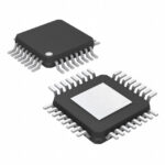 CY2DP1510AXC
The activity of extra discounts on wholesale prices is in full swing…
Please fill in your contact information and we will send you the latest wholesale price list.






