 ChipApex | Global Electronic Components Supplier
SEARCH
Search Product
Search Post
— IC芯片 | 连接器 | 传感器 | 被动器件 —
Search productSearch post
— IC芯片 | 连接器 | 传感器 | 被动器件 —
Consult the customer manager about the wholesale price.
consultation hotline:86-132-6715-2157
email:[email protected]
Contact the product manager for consultation. One-stop consultation is available.
Do you want a lower wholesale price? Please send us your inquiry and we will reply immediately.
The CY2DP814ZXC is a 1:4 clock fanout buffer manufactured by Cypress Semiconductor Corp. It features a single configurable input supporting LVDS, LVPECL, or LVTTL logic families, and provides four differential pairs of LVPECL outputs. Designed for data communications clock management, it reduces loading on the input clock source. The device operates at a maximum frequency of 450 MHz with a typical propagation delay of less than 4 ns and output-to-output skew of 85 ps. It requires a 3.3 V supply (3.135V to 3.465V) and functions within a commercial temperature range of 0°C to 70°C.
Verify the package type matches the required footprint; this part uses a 16-pin TSSOP. Confirm the ordering suffix 'X' indicates bulk tube packaging rather than tape and reel. Ensure the design supports the specified 3.3V supply voltage and commercial temperature range requirements.
Select this component when a low-skew fanout buffer is needed for LVDS or LVPECL clocks. The configurable input allows flexibility in interfacing with different logic families. Verify that the 16-TSSOP package dimensions fit the PCB layout constraints and that the 450 MHz maximum frequency meets the system timing requirements.
The CY2DP814ZXC belongs to the Cypress CY2 series of network circuits, produced using 0.35-micron CMOS technology. This specific part number denotes the lead-free version in a 16-pin TSSOP package intended for commercial temperature applications. It is part of a family designed for high-speed logic applications requiring precise clock distribution.
The CY2DP814ZXCT is a compatible alternative offering the same electrical specifications but packaged in tape and reel format instead of bulk tubes. Other variants like CY2DP814SI are available in SOIC packages if the TSSOP footprint is unsuitable.
The input receiver configuration is determined by the state of the CONFIG pin (Pin 2). A logic low selects LVDS or LVPECL, while a logic high selects LVTTL/LVCMOS.
The maximum frequency is 450 MHz under standard load conditions with a 50% duty cycle at 3.3V VDD.
Yes, for LVTTL/LVCMOS inputs, the signal can be inverted or kept true by grounding either the IN+ or IN- pin, as detailed in the function control table.
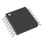 CY2DP814ZXC
The activity of extra discounts on wholesale prices is in full swing…
Please fill in your contact information and we will send you the latest wholesale price list.





