 ChipApex | Global Electronic Components Supplier
SEARCH
Search Product
Search Post
— IC芯片 | 连接器 | 传感器 | 被动器件 —
Search productSearch post
— IC芯片 | 连接器 | 传感器 | 被动器件 —
Consult the customer manager about the wholesale price.
consultation hotline:86-132-6715-2157
email:[email protected]
Contact the product manager for consultation. One-stop consultation is available.
Do you want a lower wholesale price? Please send us your inquiry and we will reply immediately.
The CY2DP818ZC is a 1:8 clock fanout buffer manufactured by Infineon Technologies (originally Cypress Semiconductor). It operates on a single 3.3V supply and supports frequencies up to 350 MHz. The device features one configurable input supporting LVDS, LVPECL, or LVTTL/LVCMOS logic levels, controlled via the InConfig pin. It provides eight differential LVPECL output pairs designed to drive 50-ohm loads. Key electrical characteristics include a typical propagation delay of 4 ns, low output skew of 0.2 ns, and an operating temperature range of 0°C to 70°C.
Verify the manufacturer origin, as the part was originally produced by Cypress Semiconductor before its acquisition by Infineon. Confirm the package type is 38-pin TSSOP and ensure the commercial temperature grade (0°C to 70°C) matches system requirements. Check for specific ordering suffixes such as 'T' for tape and reel packaging if applicable.
Select this component when a single clock source needs distribution to eight LVPECL destinations. Ensure the input signal matches the configured receiver family (LVDS, LVPECL, or LVTTL) by setting the InConfig pin correctly. Verify that the 3.3V supply voltage and 350 MHz maximum frequency align with the system's timing and power constraints.
The CY2DP818ZC belongs to the CY2DP818 series of clock fanout buffers. This series includes variants with different temperature ratings and packaging options, such as industrial grades (-40°C to 85°C) and tape-and-reel configurations. The ZC suffix specifically denotes the commercial temperature range in a tube package.
Direct replacements within the same series include CY2DP818ZI (Industrial), CY2DP818ZIT (Industrial Tape & Reel), and CY2DP818ZXI/ZXC/ZXCT (Pb-Free versions). Ensure any substitute maintains the 38-TSSOP package and compatible electrical specifications.
The input type is user-configurable via the InConfig pin (Pin 7). Setting it high selects LVTTL/LVCMOS single-ended input, while setting it low selects LVDS/LVPECL differential input.
The maximum operating frequency is 350 MHz under standard load circuit conditions with a 3.3V supply and a 45%-55% duty cycle.
The device provides eight pairs of LVPECL outputs capable of driving a 50-ohm load. The typical propagation delay is 4 ns, and the output skew between packages is typically 1 ns.
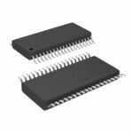 CY2DP818ZC
The activity of extra discounts on wholesale prices is in full swing…
Please fill in your contact information and we will send you the latest wholesale price list.







