 ChipApex | Global Electronic Components Supplier
SEARCH
Search Product
Search Post
— IC芯片 | 连接器 | 传感器 | 被动器件 —
Search productSearch post
— IC芯片 | 连接器 | 传感器 | 被动器件 —
Consult the customer manager about the wholesale price.
consultation hotline:86-132-6715-2157
email:[email protected]
Contact the product manager for consultation. One-stop consultation is available.
Do you want a lower wholesale price? Please send us your inquiry and we will reply immediately.
The CY2DP818ZI is a fanout buffer manufactured by Cypress Semiconductor Corp, designed for clock distribution applications. It features a single circuit with a 1:8 input-to-output ratio and supports differential signaling on both input and output sides. The device operates at a maximum frequency of 350 MHz and requires a supply voltage between 3.135V and 3.465V. Input signal compatibility includes LVDS, LVPECL, and LVTTL, while the outputs provide LVPECL signals. It is housed in a 38-TSSOP package and functions within an operating temperature range of -40°C to 85°C.
Verify the specific ordering suffix against official Cypress documentation to confirm pinout and electrical characteristics. Ensure the 38-TSSOP package dimensions align with PCB layout requirements. Confirm that the 3.135V to 3.465V supply voltage range matches the system power design. Check for RoHS compliance status if required by project specifications.
Select this component when a 1:8 split is required from LVDS, LVPECL, or LVTTL inputs to LVPECL outputs. Ensure the system can accommodate the 350 MHz maximum frequency and the specified 3.135V-3.465V supply voltage. Verify that the 38-TSSOP surface mount package fits the mechanical constraints. Consider thermal performance within the -40°C to 85°C operating range.
This part belongs to the Cypress clock buffer family, specifically designed for distributing clock signals in high-speed digital systems. It serves as a critical interface component for converting and amplifying clock sources to drive multiple downstream loads with minimal skew.
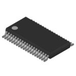 CY2DP818ZI
The activity of extra discounts on wholesale prices is in full swing…
Please fill in your contact information and we will send you the latest wholesale price list.





