 ChipApex | Global Electronic Components Supplier
SEARCH
Search Product
Search Post
— IC芯片 | 连接器 | 传感器 | 被动器件 —
Search productSearch post
— IC芯片 | 连接器 | 传感器 | 被动器件 —
Consult the customer manager about the wholesale price.
consultation hotline:86-132-6715-2157
email:[email protected]
Contact the product manager for consultation. One-stop consultation is available.
Do you want a lower wholesale price? Please send us your inquiry and we will reply immediately.
The CY2SSTV855ZXC is a high-performance, very-low-skew, zero-delay differential clock buffer and driver manufactured by Skyworks Solutions Inc. It distributes a differential SSTL_2 clock input to four differential output pairs and one feedback pair using an internal phase-locked loop (PLL). The device operates with AVDD and VDDQ supplies at 2.5V nominal. Key specifications include a low-to-high propagation delay of 1.5 ns typical, output skew under 100 ps, and half-period jitter below 100 ps for frequencies above 66 MHz. It supports Spread Spectrum Clocking (SSCG) for EMI reduction and conforms to JEDEC DDR specifications.
Verify the ordering suffix 'ZXC' corresponds to the commercial temperature range (0°C to 70°C) in the 28-pin TSSOP package. Confirm whether tape and reel packaging is required by checking for the 'CT' suffix variant. Ensure compatibility with the 2.5V supply voltage requirements specified in the datasheet.
Select this component for designs requiring a 1:5 differential clock split with minimal skew. Ensure the PCB layout allows for close placement of bypass capacitors (< 0.2”) to power pins to maintain high-frequency filtering characteristics. Verify that the input clock frequency falls within the operational range where static phase offset remains within ±450 ps.
This part belongs to the CY2SSTV855 family of differential clock buffers. The 'ZXC' suffix indicates a lead-free version in a standard commercial temperature grade. Other variants include industrial grades ('ZI') and tape-and-reel options ('CT'). The device is functionally equivalent to other members of the series but differs in temperature rating and packaging format.
Direct replacements within the same family include CY2SSTV855ZC (commercial, standard pkg), CY2SSTV855ZCT (commercial, tape & reel), CY2SSTV855ZI (industrial), and CY2SSTV855ZXI (industrial, lead-free). Ensure the substitute matches the required operating temperature range and packaging type.
It achieves near-zero delay by connecting the external feedback inputs (FBINT/FBINC) to the feedback outputs (FBOUTT/FBOUTC). The PLL aligns the output edge with the input reference edge, effectively eliminating propagation delay through the device.
When PWRDWN is HIGH, the device operates normally. When PWRDWN is LOW, all outputs are disabled to a high-impedance state, and the PLL is shut down.
Yes, the device is Spread Aware and supports tracking of spread spectrum clock inputs to reduce electromagnetic interference (EMI).
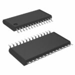 CY2SSTV855ZXC
The activity of extra discounts on wholesale prices is in full swing…
Please fill in your contact information and we will send you the latest wholesale price list.






