 ChipApex | Global Electronic Components Supplier
SEARCH
Search Product
Search Post
— IC芯片 | 连接器 | 传感器 | 被动器件 —
Search productSearch post
— IC芯片 | 连接器 | 传感器 | 被动器件 —
Consult the customer manager about the wholesale price.
consultation hotline:86-132-6715-2157
email:[email protected]
Contact the product manager for consultation. One-stop consultation is available.
Do you want a lower wholesale price? Please send us your inquiry and we will reply immediately.
The CY2SSTV857ZXI-27 is a high-performance, low-skew, low-jitter zero-delay buffer designed for distributing differential clocks in high-speed applications. It generates ten differential pair clock outputs from one differential pair clock input and features differential feedback inputs and outputs to enable near-zero delay operation in nested clock trees. The device operates at frequencies between 60 MHz and 200 MHz, supporting 266 MHz and 333 MHz DDR SDRAM standards. It functions with a 2.5V supply voltage and includes power management capabilities via a dedicated control input.
Verify the ordering suffix 'ZXI' confirms the industrial temperature range of –40° C to +85° C and lead-free status. Confirm the package type is the 48-pin TSSOP (Z48). Ensure compatibility with the specific -27 speed grade for the required frequency performance.
Select this component when a zero-delay buffer is required for DDR SDRAM clock distribution. Ensure the design supports a 2.5V nominal supply for both AVDD and VDDQ. Verify that the load capacitance requirements fall within the specified ranges for direct termination or split termination configurations.
This part belongs to the CY2SSTV857 family of differential clock buffers. The 'ZXI' suffix indicates an industrial temperature rating and lead-free construction. The '-27' designation specifies the electrical characteristics and speed grade compatible with 266/333 MHz DDR standards.
The datasheet notes pin-compatibility with CDC857-2 and -3 devices. Verify functional equivalence regarding jitter specifications and power-down behavior before substitution.
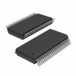 CY2SSTV857ZXI-27
The activity of extra discounts on wholesale prices is in full swing…
Please fill in your contact information and we will send you the latest wholesale price list.






