 ChipApex | Global Electronic Components Supplier
SEARCH
Search Product
Search Post
— IC芯片 | 连接器 | 传感器 | 被动器件 —
Search productSearch post
— IC芯片 | 连接器 | 传感器 | 被动器件 —
Consult the customer manager about the wholesale price.
consultation hotline:86-132-6715-2157
email:[email protected]
Contact the product manager for consultation. One-stop consultation is available.
Do you want a lower wholesale price? Please send us your inquiry and we will reply immediately.
The CY2V9950AC is a Zero Delay Buffer (ZDB) manufactured by Cypress Semiconductor Corp, designed for clock distribution applications. It features a 2:8 input-to-output ratio, accepting LVCMOS or LVTTL inputs and providing eight LVTTL outputs. The device operates within dual voltage ranges of 2.25V to 2.75V and 2.97V to 3.63V. Packaged in a 32-TQFP surface-mount case measuring 7x7 mm, it supports an operating temperature range of 0°C to 70°C. This component eliminates clock skew by feeding back the output clock to the input, ensuring minimal propagation delay.
Verify the specific suffix 'AC' against official Cypress documentation to confirm temperature grade and packaging details. Ensure compatibility with the required 2.25V–2.75V or 2.97V–3.63V power rails. Confirm that the 32-TQFP footprint matches the PCB design constraints. Check for end-of-life status if long-term production is required.
Select this component when low-skew clock distribution is critical for systems using LVTTL interfaces. The dual voltage capability allows flexibility in mixed-voltage environments. Ensure the design accommodates the 32-TQFP package dimensions. Verify that the input signal integrity meets LVCMOS/LVTTL thresholds for reliable zero-delay operation.
This part belongs to the Cypress clock buffer family, specifically optimized for zero-delay buffering. It differs from standard fanout buffers by incorporating feedback mechanisms to minimize jitter and skew. The 2:8 ratio makes it suitable for driving multiple downstream clock nodes from two primary sources.
Check for direct pin-compatible alternatives within the CY2V99xx series. Verify that any substitute maintains the same 2:8 ratio and LVTTL output characteristics. Ensure voltage and thermal specifications match the original design requirements.
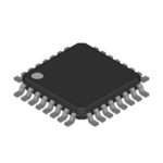 CY2V9950AC
The activity of extra discounts on wholesale prices is in full swing…
Please fill in your contact information and we will send you the latest wholesale price list.





