 ChipApex | Global Electronic Components Supplier
SEARCH
Search Product
Search Post
— IC芯片 | 连接器 | 传感器 | 被动器件 —
Search productSearch post
— IC芯片 | 连接器 | 传感器 | 被动器件 —
Consult the customer manager about the wholesale price.
consultation hotline:86-132-6715-2157
email:[email protected]
Contact the product manager for consultation. One-stop consultation is available.
Do you want a lower wholesale price? Please send us your inquiry and we will reply immediately.
The CY2X013FLXC is a low-noise LVDS clock generator manufactured by Cypress Semiconductor Corp. It utilizes a phase-locked loop (PLL) architecture with a voltage control oscillator (VCO) to achieve typical RMS phase jitter of less than 1 ps. The device accepts an external crystal reference input, nominally 25 MHz, and generates one LVDS output pair. It supports operation at both 3.3 V and 2.5 V supply voltages and features an asynchronous enable/disable function via an OE pin. The component is housed in an 8-pin TSSOP package.
Verify the specific suffix FLXC against official datasheets to confirm package type and temperature range. Ensure compatibility with existing 3.3 V or 2.5 V power rails. Confirm that the single LVDS output configuration meets the target design requirements. Check for end-of-life status as Cypress products may have transitioned to Infineon.
Select this component when low phase jitter is critical for signal integrity. The single LVDS output limits use cases to point-to-point clock distribution. Verify that the 25 MHz crystal reference frequency matches the system oscillator requirements. Consider the TSSOP package constraints for PCB layout and thermal management.
This part belongs to the CY2XL13 family of low-noise clock generators. These devices are designed to replace traditional oscillators in high-speed digital systems. The family offers configurable outputs and low jitter performance suitable for modern interface standards. Cypress Semiconductor was acquired by Infineon Technologies, affecting long-term support channels.
The maximum output clock frequency is 125 MHz.
No, the CY2X013FLXC generates only one LVDS output pair.
The output can be asynchronously enabled or disabled using the dedicated OE pin.
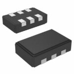 CY2X013FLXC
The activity of extra discounts on wholesale prices is in full swing…
Please fill in your contact information and we will send you the latest wholesale price list.





