 ChipApex | Global Electronic Components Supplier
SEARCH
Search Product
Search Post
— IC芯片 | 连接器 | 传感器 | 被动器件 —
Search productSearch post
— IC芯片 | 连接器 | 传感器 | 被动器件 —
Consult the customer manager about the wholesale price.
consultation hotline:86-132-6715-2157
email:[email protected]
Contact the product manager for consultation. One-stop consultation is available.
Do you want a lower wholesale price? Please send us your inquiry and we will reply immediately.
The CY7B991-2JC is a Programmable Skew Clock Buffer (PSCB) from the RoboClock series, manufactured by Cypress Semiconductor. It features an integrated Phase-Locked Loop (PLL) and provides eight TTL outputs arranged in four user-controllable pairs. The device operates within a frequency range of 3.75 MHz to 80 MHz with a supply voltage of 4.5V to 5.5V. Key electrical specifications include output pair skew less than 100 ps typical (250 ps maximum), jitter under 200 ps peak-to-peak, and zero input-to-output delay. It supports selectable skew up to 18 ns, inverted/non-inverted outputs, and frequency division/multiplication functions.
Verify the ordering suffix 'JC' corresponds to the J65 package type (32-Lead Plastic Leaded Chip Carrier) and Commercial operating temperature range (0°C to +70°C). Confirm that the specific speed grade '-2' aligns with the required 250 ps maximum skew performance. Ensure compatibility with 5V logic levels and TTL input/output requirements.
Select this component when precise timing alignment between multiple clock domains is critical. The CY7B991-2JC is suitable for designs requiring programmable skew to compensate for PCB trace length differences. Choose this part over the CMOS CY7B992 variant if TTL logic levels are required for the output drivers. Verify that the application frequency falls within the 3.75–80 MHz range supported by the FS pin configuration.
The CY7B991-2JC belongs to the CY7B991/CY7B992 family of Programmable Skew Clock Buffers. It is functionally identical to the CY7B992-2JC except for the output logic family; the CY7B991 provides TTL outputs while the CY7B992 provides CMOS outputs. Both share the same internal PLL architecture, pinout, and control logic.
Public confirmed substitute part numbers: CY7B992-2JC (CMOS output version).
The skew range is defined by time units (tU) derived from the operating frequency and the FS pin setting. Outputs can be skewed up to ±6 time units from their nominal position, allowing for total skew adjustments of up to 18 ns.
The TEST pin controls the internal PLL. When tied LOW (normal operation), the PLL synchronizes the REF and FB inputs. If forced to MID or HIGH states, the PLL disconnects, and REF input levels directly control all outputs.
Yes. By connecting a divided output (divide-by-two or divide-by-four) to the FB input, the internal PLL multiplies the reference frequency at the REF input by two or four at the undivided outputs.
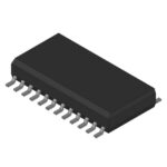 CY7B991-2JC
The activity of extra discounts on wholesale prices is in full swing…
Please fill in your contact information and we will send you the latest wholesale price list.






