 ChipApex | Global Electronic Components Supplier
SEARCH
Search Product
Search Post
— IC芯片 | 连接器 | 传感器 | 被动器件 —
Search productSearch post
— IC芯片 | 连接器 | 传感器 | 被动器件 —
Consult the customer manager about the wholesale price.
consultation hotline:86-132-6715-2157
email:[email protected]
Contact the product manager for consultation. One-stop consultation is available.
Do you want a lower wholesale price? Please send us your inquiry and we will reply immediately.
The CY7B991V-2JCT is a low-voltage programmable skew clock buffer from the RoboClock series, manufactured by Cypress Semiconductor. It operates on a single 3.3 V supply and supports output frequencies between 3.75 MHz and 80 MHz. The device features eight outputs arranged in four pairs within a 32-pin PLCC package. Key electrical characteristics include zero input-to-output delay, 50% duty cycle outputs, and typical output pair skew of less than 100 ps. It integrates a phase-locked loop to cancel external load delays.
Verify the specific -2 speed grade against system timing requirements, as it differs from the standard -5 option in propagation delay and skew specifications. Confirm that the 32-pin PLCC package aligns with the target PCB footprint. Check for RoHS compliance status relative to current manufacturing standards.
Select this component when precise control over output timing skew is required alongside frequency multiplication or division. Ensure the operating frequency falls within the 3.75 MHz to 80 MHz range defined by the FS pin configuration. Verify that the LVTTL output levels are compatible with the receiving logic inputs.
This part belongs to the CY7B991V family of low-voltage programmable skew clock buffers. It shares functional similarities with the CY7B9911V but is optimized for 3.3 V operation. The -2 suffix denotes a specific speed grade variant within the product line, distinct from the -5 or -7 options found in other datasheet revisions.
Publicly confirmed substitute part numbers are not available in the provided documentation. Designers should verify compatibility with any alternative clock buffers regarding voltage levels, package dimensions, and skew performance metrics.
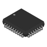 CY7B991V-2JCT
The activity of extra discounts on wholesale prices is in full swing…
Please fill in your contact information and we will send you the latest wholesale price list.





