 ChipApex | Global Electronic Components Supplier
SEARCH
Search Product
Search Post
— IC芯片 | 连接器 | 传感器 | 被动器件 —
Search productSearch post
— IC芯片 | 连接器 | 传感器 | 被动器件 —
Consult the customer manager about the wholesale price.
consultation hotline:86-132-6715-2157
email:[email protected]
Contact the product manager for consultation. One-stop consultation is available.
Do you want a lower wholesale price? Please send us your inquiry and we will reply immediately.
The CY7B992-2JCT is a programmable skew clock buffer manufactured by Cypress Semiconductor Corp. It operates as a fanout distribution and zero delay buffer with one circuit, providing an input-to-output ratio of 1:8. The device accepts CMOS inputs and generates CMOS outputs, supporting a supply voltage range of 4.5V to 5.5V. It is housed in a 32-LCC (J-Lead) surface-mount package, specifically the 32-PLCC form factor measuring 11.43x13.97 mm. The component is designed for commercial applications within an operating temperature range of 0°C to 70°C.
Verify the specific suffix 'JCT' against official Cypress documentation to confirm if it denotes tape-and-reel packaging or other handling variations distinct from the bulk 'JC' variant. Confirm end-of-life status and lead-free compliance requirements prior to procurement planning.
Select this component when precise control over output skew is required alongside zero-delay buffering capabilities. Ensure the design environment supports the specified 4.5V to 5.5V supply voltage and that the 32-PLCC package fits the available PCB footprint constraints.
This part belongs to the CY7B991/CY7B992 family of programmable skew clock buffers. These devices are engineered to provide multiple output drivers arranged in pairs, allowing system designers to optimize timing margins in complex digital architectures through selectable skew and frequency multiplication options.
The QS5992-5JRX is documented as pin-compatible with the CY7B992 series. Verify electrical parameter alignment, particularly regarding drive strength and skew specifications, before substituting.
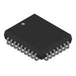 CY7B992-2JCT
The activity of extra discounts on wholesale prices is in full swing…
Please fill in your contact information and we will send you the latest wholesale price list.





