 ChipApex | Global Electronic Components Supplier
SEARCH
Search Product
Search Post
— IC芯片 | 连接器 | 传感器 | 被动器件 —
Search productSearch post
— IC芯片 | 连接器 | 传感器 | 被动器件 —
Consult the customer manager about the wholesale price.
consultation hotline:86-132-6715-2157
email:[email protected]
Contact the product manager for consultation. One-stop consultation is available.
Do you want a lower wholesale price? Please send us your inquiry and we will reply immediately.
The CY7B992-7JC is a programmable skew clock buffer manufactured by Cypress Semiconductor Corp. It features eight CMOS outputs arranged in four pairs, providing user-selectable control over system clock functions to optimize timing in high-performance computer systems. Each driver pair can terminate transmission lines with impedances as low as 50Ω. The device operates within an output frequency range of 3.75 MHz to 80 MHz and delivers minimal specified output skews with full-swing logic levels. It includes selectable skew up to 18 ns, inverted/non-inverted options, and frequency multiplication/division capabilities (1/4, 1/2, 2x, 4x).
Verify the package type matches the 32-LCC (J-Lead) specification. Confirm the manufacturer is Cypress Semiconductor Corp. Ensure the operating temperature range requirements are met for the specific application environment. Check for lead-free compliance if required by local regulations.
Select this component when precise clock skew management is critical for system performance. The CY7B992-7JC is suitable for designs requiring multiple clock phases derived from a single source. Consider the 50Ω termination capability if driving long traces or high-speed buses. Verify that the 3.75 MHz to 80 MHz frequency range covers the system's operational needs.
This part belongs to the CY7B991/CY7B992 Programmable Skew Clock Buffer family. The CY7B992 variant specifically provides CMOS outputs, whereas the CY7B991 offers TTL outputs. Both share similar functional architectures for optimizing system timing through programmable skew and frequency multiplication.
The QS5992 series is pin-compatible with the CY7B992. Verify voltage levels and skew specifications against the QS5992 datasheet before substitution. Ensure the replacement supports the required 50Ω termination and frequency range.
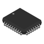 CY7B992-7JC
The activity of extra discounts on wholesale prices is in full swing…
Please fill in your contact information and we will send you the latest wholesale price list.





