ChipApex | Global Electronic Components Supplier

SEARCH
Search Product
Search Post
— IC芯片 | 连接器 | 传感器 | 被动器件 —
Search productSearch post
— IC芯片 | 连接器 | 传感器 | 被动器件 —
Consult the customer manager about the wholesale price.
consultation hotline:86-132-6715-2157
email:[email protected]
Contact the product manager for consultation. One-stop consultation is available.
Do you want a lower wholesale price? Please send us your inquiry and we will reply immediately.
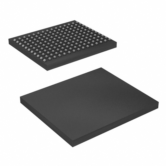
CY7C1168KV18-400BZXC is listed in the Memory IC range at ChipApex. The manufacturer field lists Infineon Technologies. Its product description is IC SRAM 18MBIT PARALLEL 165FBGA. Review the specifications below when checking this part for your BOM.
The CY7C1168KV18-400BZXC is an 18-Mbit DDR II+ synchronous SRAM with a 1M x 18 organization. It supports a maximum operating frequency of 400 MHz and operates within a voltage range of 1.7 V to 1.9 V. The device features a two-word burst architecture with 2.5 cycle read latency when the DOFF pin is asserted HIGH. It utilizes a parallel interface and is housed in a 165-ball FBGA package.
Verify the specific speed grade suffix matches the required 400 MHz operational frequency. Confirm the package type corresponds to the 165-ball FBGA configuration. Ensure the ordering suffix aligns with the desired lead-free finish and commercial temperature range specifications before finalizing procurement orders.
Select this component for designs requiring pipelined synchronous SRAM with DDR II+ architecture. It is suitable for applications needing reduced address bus frequencies through burst operations. Consider the 2.5-cycle read latency and the requirement for separate K and K input clocks for proper timing alignment.
This part belongs to the Infineon DDR II+ SRAM family, which includes variants like the CY7C1170KV18. These devices are designed for high-speed data processing using advanced 65nm technology. The family emphasizes high bandwidth and precise timing control through dedicated clock inputs and echo outputs.
Public confirmed substitute part numbers: None identified in source material.
Explore related parts through Memory, Integrated Circuits (ICs), all product categories, ChipApex homepage.
 CY7C1168KV18-400BZXC

The activity of extra discounts on wholesale prices is in full swing…
Please fill in your contact information and we will send you the latest wholesale price list.