ChipApex | Global Electronic Components Supplier

SEARCH
Search Product
Search Post
— IC芯片 | 连接器 | 传感器 | 被动器件 —
Search productSearch post
— IC芯片 | 连接器 | 传感器 | 被动器件 —
Consult the customer manager about the wholesale price.
consultation hotline:86-132-6715-2157
email:[email protected]
Contact the product manager for consultation. One-stop consultation is available.
Do you want a lower wholesale price? Please send us your inquiry and we will reply immediately.
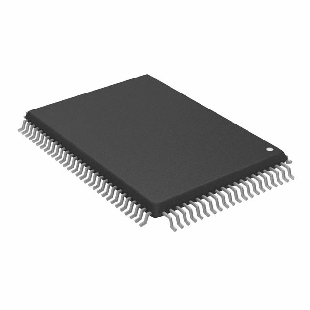
CY7C1345G-100AXCT is listed in the Memory IC range at ChipApex. The manufacturer field lists Infineon Technologies. Its product description is IC SRAM 4.5MBIT PAR 100TQFP. Review the specifications below when checking this part for your BOM.
The CY7C1345G-100AXCT is a 4-Mbit (128K × 36) synchronous static random-access memory manufactured by Infineon Technologies. It features an 8.0 ns maximum access time and supports a 100 MHz clock frequency. The device utilizes a 100-pin TQFP package with surface-mount installation. Electrical specifications include a 3.3 V core supply voltage range of 3.135 V to 3.6 V, and a 2.5 V or 3.3 V I/O supply. Maximum operating current is 205 mA, while maximum standby current is 40 mA. The industrial temperature rating spans from -40 °C to +85 °C.
Verify component authenticity through authorized distribution channels due to potential counterfeit risks. Confirm that the ZZ pin is externally connected to ground as required by silicon errata documentation. Ensure power supply sequencing meets specified ramp-up requirements before initiating read or write operations to maintain data integrity.
Select this component when interfacing with processors requiring a 36-bit data width and synchronous flow-through architecture. Verify that the system design accommodates the specific 100-pin TQFP footprint and thermal resistance characteristics. Confirm that the available 2.5 V or 3.3 V I/O supply aligns with the target logic levels.
This part belongs to the CY7C1345G family of 4-Mbit synchronous SRAMs. It shares architectural similarities with other members like the CY7C1345G-100AXI but differs in packaging and termination specifications. The series is designed for low-glue-logic integration with high-speed CPUs.
Direct substitutes within the same family include CY7C1345G-100AXI and CY7C1345G-100AXC. Cross-family replacements require verification of pinout compatibility and electrical parameter alignment.
The burst sequence is selected by the MODE input pin. A LOW level selects a linear burst sequence, while a HIGH level or floating state selects an interleaved burst sequence.
The ZZ pin is an asynchronous sleep input. Asserting it places the device in a non-time critical sleep condition with data integrity preserved. Errata requires this pin to be externally connected to ground during normal operation.
Explore related parts through Memory, Integrated Circuits (ICs), all product categories, ChipApex homepage.
 CY7C1345G-100AXCT

The activity of extra discounts on wholesale prices is in full swing…
Please fill in your contact information and we will send you the latest wholesale price list.