 ChipApex | Global Electronic Components Supplier

SEARCH
Search Product
Search Post
— IC芯片 | 连接器 | 传感器 | 被动器件 —
Search productSearch post
— IC芯片 | 连接器 | 传感器 | 被动器件 —
Consult the customer manager about the wholesale price.
consultation hotline:86-132-6715-2157
email:[email protected]
Contact the product manager for consultation. One-stop consultation is available.
Do you want a lower wholesale price? Please send us your inquiry and we will reply immediately.
CY7C1383D-133AXIT is listed in the Memory IC range at ChipApex. The manufacturer field lists Infineon Technologies. Its product description is IC SRAM 18MBIT PARALLEL 100TQFP. Review the specifications below when checking this part for your BOM.
The CY7C1383D-133AXIT is a 18-Mbit (1M x 18) synchronous flow-through static random-access memory manufactured by Infineon Technologies. It supports bus operations at a maximum clock frequency of 133 MHz with a fast clock-to-output access time of 6.5 ns. The device operates from a 3.3V core power supply and accepts 2.5V or 3.3V IO supplies. It features an asynchronous output enable, user-selectable burst counter for linear or interleaved sequences, and separate processor and controller address strobes. The component is housed in a 100-pin TQFP package.
Verify the specific suffix AXIT against official documentation to confirm packaging type and RoHS compliance status. Confirm that the 100-pin TQFP package matches the required footprint. Ensure the 133 MHz speed grade aligns with system timing requirements. Check for any discontinuation notices as this series may have limited availability.
Select this component when a 1M x 18 organization is required for synchronous applications. The 133 MHz speed grade provides a 6.5 ns access time suitable for high-frequency buses. Verify compatibility with 3.3V core and 2.5V/3.3V IO voltage levels. Consider the 100-pin TQFP package constraints for PCB layout and thermal management.
This part belongs to the CY7C1381/CY7C1383 family of 18-Mbit synchronous SRAMs. The 'D' designation indicates the 100-pin TQFP or 165-ball FBGA package option, while 'F' denotes the 119-ball BGA. The '133' specifies the 133 MHz speed bin. These devices are designed to interface directly with high-speed processors with minimal glue logic.
CY7C1383KV33-133AXI
The burst sequence is selected via the MODE input pin. A LOW level selects a linear burst sequence, while a HIGH level or floating state selects an interleaved burst sequence compatible with Intel Pentium processors.
The ZZ pin is an asynchronous sleep input. Asserting it HIGH places the device into a non-time critical sleep mode with data integrity preserved. Two clock cycles are required to enter or exit this mode.
Explore related parts through Memory, Integrated Circuits (ICs), all product categories, ChipApex homepage.
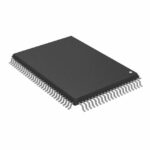 CY7C1383D-133AXIT

The activity of extra discounts on wholesale prices is in full swing…
Please fill in your contact information and we will send you the latest wholesale price list.





