 ChipApex | Global Electronic Components Supplier

SEARCH
Search Product
Search Post
— IC芯片 | 连接器 | 传感器 | 被动器件 —
Search productSearch post
— IC芯片 | 连接器 | 传感器 | 被动器件 —
Consult the customer manager about the wholesale price.
consultation hotline:86-132-6715-2157
email:[email protected]
Contact the product manager for consultation. One-stop consultation is available.
Do you want a lower wholesale price? Please send us your inquiry and we will reply immediately.
CY7C1423BV18-250BZC is listed in the Memory IC range at ChipApex. The manufacturer field lists Cypress Semiconductor Corp. Its product description is IC SRAM 36MBIT PAR 165FBGA. Review the specifications below when checking this part for your BOM.
The CY7C1423BV18 is a 36-Mbit Double Data Rate Separate I/O (DDR-II SIO) synchronous pipelined SRAM manufactured by Cypress Semiconductor. It features a 2M x 18 memory organization and supports clock frequencies up to 300 MHz, enabling data transfer rates of 600 MHz. The device utilizes a two-word burst architecture to reduce address bus frequency requirements. It operates with a 1.8V core power supply and includes HSTL inputs and outputs. The component is available in a 165-ball FBGA package measuring 15 x 17 x 1.4 mm.
Verify the specific speed grade required for the target application, as performance metrics vary across the product family. Confirm whether lead-free or non-lead-free packaging is necessary, as both options are offered. Ensure that the system design accommodates the 165-ball FBGA footprint dimensions. Validate that the power supply rails meet the specified 1.8V core voltage requirements before integration.
Select this component when a 36-Mbit capacity with a 2M x 18 organization is required. Choose this part over other variants if the specific DDR-II SIO architecture with separate input and output clocks is preferred for minimizing skew. Consider the 300 MHz maximum operating frequency if higher bandwidth than lower speed grades provides. Ensure the design supports the necessary DLL configuration and impedance matching via the ZQ pin.
This device belongs to the CY7C142x series of DDR-II SIO SRAMs from Cypress Semiconductor. The series includes CY7C1422BV18 (4M x 8), CY7C1429BV18 (4M x 9), and CY7C1424BV18 (1M x 36). All members share the same physical package, pinout structure, and core architectural features, differing primarily in memory density and data width organization.
Direct replacements within the same package and architecture include CY7C1422BV18, CY7C1429BV18, and CY7C1424BV18. These parts share identical pinouts and functional descriptions but differ in memory organization (x8, x9, or x36). Verify that the system address decoding and data bus width can accommodate the alternative organization.
When the DLL is enabled (DOFF pin tied HIGH), the device operates with a 1.5-cycle read latency. If the DLL is disabled (DOFF pin connected to VSS), it behaves like a DDR-I device with a 1-cycle read latency.
The ZQ pin is used for output impedance matching. An external resistor (RQ) must be connected between ZQ and ground to tune the output drivers. The value of RQ should be 5 times the intended line impedance, typically ranging from 175 Ω to 350 Ω.
Yes, the device supports a single clock mode where the same input clocks (K/K) control both input and output registers. This is achieved by tying the output clocks (C/C) HIGH at power on.
Explore related parts through Memory, Integrated Circuits (ICs), all product categories, ChipApex homepage.
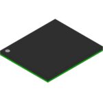 CY7C1423BV18-250BZC

The activity of extra discounts on wholesale prices is in full swing…
Please fill in your contact information and we will send you the latest wholesale price list.





