ChipApex | Global Electronic Components Supplier

SEARCH
Search Product
Search Post
— IC芯片 | 连接器 | 传感器 | 被动器件 —
Search productSearch post
— IC芯片 | 连接器 | 传感器 | 被动器件 —
Consult the customer manager about the wholesale price.
consultation hotline:86-132-6715-2157
email:[email protected]
Contact the product manager for consultation. One-stop consultation is available.
Do you want a lower wholesale price? Please send us your inquiry and we will reply immediately.
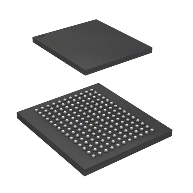
CY7C1425JV18-250BZC is listed in the Memory IC range at ChipApex. The manufacturer field lists Cypress Semiconductor Corp. Its product description is IC SRAM 36MBIT PAR 165FBGA. Review the specifications below when checking this part for your BOM.
The CY7C1425JV18-250BZC is a 36-Mbit QDR-II SRAM with a 4M x 9 organization. It operates at a maximum clock frequency of 250 MHz, delivering data at 500 MHz via double data rate interfaces on both read and write ports. The device features separate independent read and write data ports to support concurrent transactions without bus turnaround. It utilizes a single multiplexed address input bus for both ports and includes echo clocks (CQ/CQ) to simplify high-speed system design. The core voltage is 1.8V ±0.1V, while I/O voltage ranges from 1.4V to VDD.
Verify the specific suffix 'JV18' against official Cypress/Infineon documentation to confirm it denotes the 250 MHz speed grade and Pb-free package variant. Ensure the ordering code matches the exact 165-ball FBGA configuration required for your PCB footprint. Cross-reference the manufacturer's latest datasheet revision to confirm current status and any potential obsolescence notices associated with this component family.
Select this component when a 36-Mbit capacity with a 4M x 9 word width is required for QDR-II applications. It is suitable for designs demanding 250 MHz operation with independent read and write ports. Consider the 165-ball FBGA package dimensions and the 1.8V core voltage requirement. Ensure the system supports the necessary HSTL I/O standards and provides the required reference voltage for impedance matching.
This part belongs to the CY7C14xxJV18 family of 36-Mbit QDR-II SRAMs. Other members include CY7C1410JV18 (4M x 8), CY7C1412JV18 (2M x 18), and CY7C1414JV18 (1M x 36). All share the same QDR-II architecture, 165-ball FBGA package, and general functional characteristics, differing primarily in data width and internal array organization.
CY7C1425KV18-250BZC is a documented substitute within the same product family, offering identical functionality and pinout compatibility.
Explore related parts through Memory, Integrated Circuits (ICs), all product categories, ChipApex homepage.
 CY7C1425JV18-250BZC

The activity of extra discounts on wholesale prices is in full swing…
Please fill in your contact information and we will send you the latest wholesale price list.