ChipApex | Global Electronic Components Supplier

SEARCH
Search Product
Search Post
— IC芯片 | 连接器 | 传感器 | 被动器件 —
Search productSearch post
— IC芯片 | 连接器 | 传感器 | 被动器件 —
Consult the customer manager about the wholesale price.
consultation hotline:86-132-6715-2157
email:[email protected]
Contact the product manager for consultation. One-stop consultation is available.
Do you want a lower wholesale price? Please send us your inquiry and we will reply immediately.
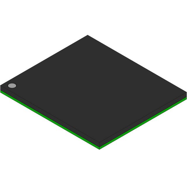
CY7C1512V18-200BZI is listed in the Memory IC range at ChipApex. The manufacturer field lists Cypress Semiconductor Corp. Its product description is IC SRAM 72MBIT PARALLEL 165FBGA. Review the specifications below when checking this part for your BOM.
The CY7C1512V18-200BZI is a 72-Mbit QDR-II SRAM with a 4M x 18 organization. It supports a maximum operating frequency of 200 MHz and utilizes a 2-word burst architecture for high bandwidth. The device features separate independent read and write data ports, enabling concurrent transactions without bus turnaround. It operates with a core voltage (VDD) of 1.8V and an I/O voltage (VDDQ) ranging from 1.4V to VDD. The component is housed in a 165-ball FBGA package measuring 15 x 17 x 1.4 mm.
Verify the specific speed grade suffix '200' matches the required 200 MHz operational frequency. Confirm the 'BZI' suffix indicates the correct lead-free packaging and commercial temperature range specifications. Ensure the 165-ball FBGA footprint aligns with the target PCB layout constraints before finalizing procurement orders.
Select this component when a 72-Mbit capacity with a 18-bit word width is required. Choose the 200 MHz variant if the system clock does not exceed this limit. Consider the QDR-II architecture for designs needing full-duplex data transfer without bus contention. Verify that the 1.8V core voltage supply is available for the target application environment.
This part belongs to the Cypress Semiconductor QDR-II SRAM family, which includes variants like the CY7C1510V18 and CY7C1514V18. These devices share the same pipelined burst architecture and physical package dimensions but differ in memory density and data bus width configurations.
CY7C1512KV18-200BZI
Address inputs are multiplexed for both ports. Read addresses are latched on the rising edge of the positive input clock (K), while write addresses are latched on the rising edge of the negative input clock (K#).
The DOFF pin is used to disable the internal Delay Lock Loop (DLL). Connecting this pin to ground turns off the DLL, altering the device's timing characteristics.
Explore related parts through Memory, Integrated Circuits (ICs), all product categories, ChipApex homepage.
 CY7C1512V18-200BZI

The activity of extra discounts on wholesale prices is in full swing…
Please fill in your contact information and we will send you the latest wholesale price list.