ChipApex | Global Electronic Components Supplier

SEARCH
Search Product
Search Post
— IC芯片 | 连接器 | 传感器 | 被动器件 —
Search productSearch post
— IC芯片 | 连接器 | 传感器 | 被动器件 —
Consult the customer manager about the wholesale price.
consultation hotline:86-132-6715-2157
email:[email protected]
Contact the product manager for consultation. One-stop consultation is available.
Do you want a lower wholesale price? Please send us your inquiry and we will reply immediately.
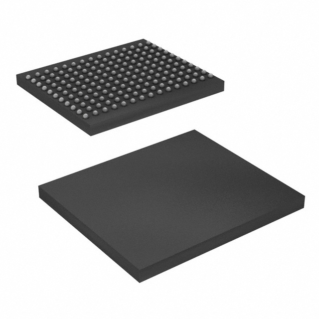
CY7C1550KV18-450BZXI is listed in the Memory IC range at ChipApex. The manufacturer field lists Infineon Technologies. Its product description is IC SRAM 72MBIT PAR 165FBGA. Review the specifications below when checking this part for your BOM.
The CY7C1550KV18-450BZXI is a 72-Mbit DDR II+ Synchronous Pipelined SRAM organized as 2M x 36. It supports a maximum clock frequency of 450 MHz, enabling data transfer rates up to 900 MHz via double data rate interfaces. The device features a two-word burst architecture with 2.0 cycle read latency when the DOFF pin is asserted HIGH. It operates with a core voltage (VDD) of 1.8 V ± 0.1 V and an I/O supply (VDDQ) ranging from 1.4 V to VDD. Maximum operating current is 820 mA for the ×36 configuration.
Verify the specific ordering suffix BZXI against the manufacturer's official documentation to confirm package type and lead-free status. Ensure the design accommodates the required VDDQ range of 1.4 V to VDD and implements proper ZQ termination for impedance matching. Confirm compatibility with the 165-ball FBGA footprint dimensions of 13 × 15 × 1.4 mm during PCB layout.
Select this component for applications requiring 72-Mbit density with a 36-bit data width. It is suitable for designs needing 450-MHz operation with 2.0-cycle read latency. Consider the CY7C1548KV18 if a 18-bit data width is preferred instead. Ensure the system supports the necessary dual-clock input requirements for DDR II+ timing.
This part belongs to the Cypress/Infineon DDR II+ SRAM family, which combines SRAM core speed with advanced synchronous peripheral circuitry. It utilizes a 65-nm technology node to achieve high performance and low power consumption compared to previous generations. The device is designed for read-intensive functions where high bandwidth and low latency are critical.
The CY7C1548KV18 is a compatible alternative within the same datasheet offering identical electrical characteristics but organized as 4M x 18 instead of 2M x 36. Verify pinout compatibility and software logic adjustments for the different data width before substitution.
When the DOFF pin is asserted HIGH, the device operates with a 2.0 cycle read latency. When DOFF is asserted LOW, it behaves like a DDR I device with a 1 cycle read latency.
The ZQ pin is used for output impedance matching. An external resistor connected between ZQ and ground tunes the output drivers to match the system data bus impedance.
Explore related parts through Memory, Integrated Circuits (ICs), all product categories, ChipApex homepage.
 CY7C1550KV18-450BZXI

The activity of extra discounts on wholesale prices is in full swing…
Please fill in your contact information and we will send you the latest wholesale price list.