ChipApex | Global Electronic Components Supplier

SEARCH
Search Product
Search Post
— IC芯片 | 连接器 | 传感器 | 被动器件 —
Search productSearch post
— IC芯片 | 连接器 | 传感器 | 被动器件 —
Consult the customer manager about the wholesale price.
consultation hotline:86-132-6715-2157
email:[email protected]
Contact the product manager for consultation. One-stop consultation is available.
Do you want a lower wholesale price? Please send us your inquiry and we will reply immediately.
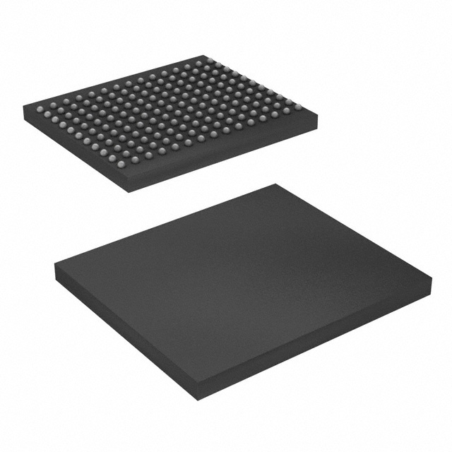
CY7C1564XV18-450BZXC is listed in the Memory IC range at ChipApex. The manufacturer field lists Infineon Technologies. Its product description is IC SRAM 72MBIT PAR 165FBGA. Review the specifications below when checking this part for your BOM.
The CY7C1564XV18 is a 72-Mbit QDR II+ Xtreme Synchronous Pipelined SRAM organized as 2M x 36. It features a maximum operating frequency of 450 MHz with double data rate interfaces on both read and write ports, enabling data transfer at 900 MHz. The device utilizes a two-word burst architecture with 2.5 cycle read latency when the DOFF pin is asserted HIGH. Core voltage (VDD) operates between 1.7 V and 1.9 V, while I/O voltage (VDDQ) ranges from 1.4 V to 1.6 V. It is housed in a 165-ball FBGA package measuring 13 x 15 x 1.4 mm.
Verify component authenticity by checking manufacturer markings against official datasheet specifications. Confirm package integrity and lead condition prior to installation. Ensure supply chain sources provide traceability documentation. Validate electrical parameters match the required operational range for your specific system design constraints.
Select this model for applications demanding high throughput with independent port access. The 2M x 36 organization suits wide-data path architectures. Consider the 2.5-cycle latency for standard operation or disable the PLL for QDR-I compatibility if lower speeds are sufficient. Ensure power supplies meet the strict core and I/O voltage tolerances specified.
This component belongs to the QDR II+ Xtreme family of synchronous SRAMs. It shares architectural similarities with the CY7C1562XV18 but differs in data width configuration. The series is designed for high-performance embedded memory solutions where deterministic access times and high bandwidth are critical system requirements.
Direct substitutes within the same density and speed class include the CY7C1562XV18 for 18-bit width applications. Verify pinout compatibility and voltage levels before swapping. Cross-referencing with other QDR II+ devices requires careful evaluation of burst architecture and latency settings.
Explore related parts through Memory, Integrated Circuits (ICs), all product categories, ChipApex homepage.
 CY7C1564XV18-450BZXC

The activity of extra discounts on wholesale prices is in full swing…
Please fill in your contact information and we will send you the latest wholesale price list.