 ChipApex | Global Electronic Components Supplier

SEARCH
Search Product
Search Post
— IC芯片 | 连接器 | 传感器 | 被动器件 —
Search productSearch post
— IC芯片 | 连接器 | 传感器 | 被动器件 —
Consult the customer manager about the wholesale price.
consultation hotline:86-132-6715-2157
email:[email protected]
Contact the product manager for consultation. One-stop consultation is available.
Do you want a lower wholesale price? Please send us your inquiry and we will reply immediately.
CY7C4251-10JXC is listed in the FIFOs Memory range at ChipApex. The manufacturer field lists Infineon Technologies. Its product description is IC FIFO SYNC 8KX9 8NS 32PLCC. Review the specifications below when checking this part for your BOM.
The CY7C4251-10JXC is a high-speed, low-power synchronous FIFO memory with an 8K x 9 organization. It operates at frequencies up to 100 MHz with a 10 ns cycle time. The device features fully asynchronous and simultaneous read/write capabilities controlled by independent clocks. It includes programmable Almost Empty and Almost Full flags for precise buffer management. The component is housed in a 32-pin PLCC package and supports width expansion.
Verify the specific suffix 'JXC' indicates Pb-free packaging as documented in the selection guide. Confirm the '-10' speed grade corresponds to the 100 MHz maximum frequency specification. Ensure the PLCC package type matches the target PCB footprint requirements. Cross-reference the density against other CY7C42X1 variants if different storage depths are required.
Select this model for applications requiring 8K depth with 9-bit data width. Choose the -10 speed grade for designs operating at or below 100 MHz. Consider the Industrial temperature range variant if ambient conditions exceed commercial limits. Evaluate width expansion needs to determine if single or multiple devices are optimal for system architecture.
This component belongs to the CY7C42X1 family of synchronous FIFOs manufactured by Cypress Semiconductor, now part of Infineon Technologies. The family offers various densities ranging from 64 to 8K words. These devices utilize advanced CMOS technology to provide high performance with low power consumption, serving as standard solutions for data buffering in digital systems.
Pin-compatible and functionally equivalent replacements include IDT72421, IDT72201, IDT72211, IDT72221, IDT72231, and IDT72241. Verify electrical characteristics and timing parameters match the original design requirements before substitution.
These flags are configured by holding WEN2/LD LOW during reset and using WCLK to write offset values into the internal registers. The default offset value is typically set to 7 words.
Yes, the device supports fully asynchronous operation where the Read Clock (RCLK) and Write Clock (WCLK) can run independently or be tied together for single-clock operation.
Explore related parts through Logic, Integrated Circuits (ICs), all product categories, ChipApex homepage.
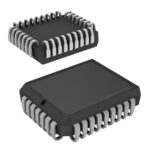 CY7C4251-10JXC

The activity of extra discounts on wholesale prices is in full swing…
Please fill in your contact information and we will send you the latest wholesale price list.





