 ChipApex | Global Electronic Components Supplier
SEARCH
Search Product
Search Post
— IC芯片 | 连接器 | 传感器 | 被动器件 —
Search productSearch post
— IC芯片 | 连接器 | 传感器 | 被动器件 —
Consult the customer manager about the wholesale price.
consultation hotline:86-132-6715-2157
email:[email protected]
Contact the product manager for consultation. One-stop consultation is available.
Do you want a lower wholesale price? Please send us your inquiry and we will reply immediately.
The CY8C20140-LDX2IT is a member of the PSoC™ 2 family, integrating an M8C 8-bit CPU with 32 kByte of Flash memory and 2 kByte of SRAM. It features programmable analog blocks including comparators and op-amps, alongside configurable digital logic. The device supports multiple communication interfaces such as UART, SPI, and I2C through its Universal Digital Block (UDB). Designed for industrial and consumer applications, it operates within a voltage range of 1.8 V to 5.5 V and supports temperatures from -40 °C to +85 °C.
Verify the specific suffix LDX2IT against official Infineon documentation to confirm package type and temperature grade. Ensure compatibility with existing design constraints before procurement. Cross-reference part numbers with current availability lists from authorized distributors to avoid obsolete stock.
Select this component when an 8-bit MCU with mixed-signal capabilities is required. Consider the limited pin count and memory size relative to more advanced PSoC families. Evaluate power consumption requirements against the operating voltage range. Confirm that the available GPIOs meet interface needs without external multiplexers.
This part belongs to the legacy PSoC 2 series, which predates the Cortex-M based PSoC 4 and 5LP families. It utilizes the M8C core architecture. While functionally similar in concept to newer devices, software libraries and peripheral configurations are not directly compatible. It serves niche applications where cost or specific legacy support is prioritized over high-performance computing.
Direct pin-to-pin replacements may be limited due to the age of the PSoC 2 platform. Review Infineon's obsolescence notices. Newer designs often migrate to PSoC 4 or PSoC 6 for better performance and toolchain support. Verify if any updated equivalents exist within the same product line.
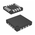 CY8C20140-LDX2IT
The activity of extra discounts on wholesale prices is in full swing…
Please fill in your contact information and we will send you the latest wholesale price list.







