 ChipApex | Global Electronic Components Supplier
SEARCH
Search Product
Search Post
— IC芯片 | 连接器 | 传感器 | 被动器件 —
Search productSearch post
— IC芯片 | 连接器 | 传感器 | 被动器件 —
Consult the customer manager about the wholesale price.
consultation hotline:86-132-6715-2157
email:[email protected]
Contact the product manager for consultation. One-stop consultation is available.
Do you want a lower wholesale price? Please send us your inquiry and we will reply immediately.
The CYW256OXC is a 12-output buffer designed for distributing high-speed clocks in PC applications. It supports up to two DDR DIMMs or three SDRAM DIMMs and includes an additional feedback output. The device features low skew outputs of less than 100 ps and operates at frequencies up to 333 MHz DDR SDRAM. It utilizes an SMBus interface for individual output control and includes a dedicated pin for power management. The component is housed in a space-saving 28-pin SSOP package.
Verify the manufacturer designation, as the datasheet identifies Silicon Laboratories Inc. while distributor listings may reference Skyworks Solutions. Confirm the specific ordering suffix (e.g., OXC vs. OXCT) determines bulk versus tape-and-reel packaging. Ensure compatibility with the required 2.5V or 3.3V supply voltage based on the target memory mode.
Select the CYW256OXC when a single-input, multi-output clock distribution solution is required for legacy DDR or SDRAM architectures. The device requires connection to either a 2.5V supply for DDR-ONLY mode or a 3.3V supply for STANDARD SDRAM mode via the VDD3.3_2.5 pins. Designers must account for the SMBus address (1101001) for configuration.
The CYW256OXC is the lead-free commercial variant of the W256 series. It is functionally equivalent to the W256H and W256HT but adheres to RoHS-compliant manufacturing standards. The part is categorized under Clock Buffers within the Clock & Timer ICs subcategory.
The W256H and W256HT are direct functional equivalents from the same manufacturer family. Verify that any substitute maintains the 28-pin SSOP footprint and compatible SMBus addressing if system integration is required.
The SEL_DDR pin configures the mode. Pulling it HIGH enables DDR-ONLY mode (requiring 2.5V supply), while pulling it LOW enables STANDARD SDRAM mode (requiring 3.3V supply).
The maximum output-to-output skew is 100 ps when all outputs are equally loaded.
Outputs are controlled via the SMBus interface using Byte 6 and Byte 7 registers, which allow each output to be set to Active (1) or Inactive (0).
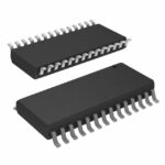 CYW256OXC
The activity of extra discounts on wholesale prices is in full swing…
Please fill in your contact information and we will send you the latest wholesale price list.





