 ChipApex | Global Electronic Components Supplier
SEARCH
Search Product
Search Post
— IC芯片 | 连接器 | 传感器 | 被动器件 —
Search productSearch post
— IC芯片 | 连接器 | 传感器 | 被动器件 —
Consult the customer manager about the wholesale price.
consultation hotline:86-132-6715-2157
email:[email protected]
Contact the product manager for consultation. One-stop consultation is available.
Do you want a lower wholesale price? Please send us your inquiry and we will reply immediately.
The CYW256OXCT is a 12-output clock buffer designed for distributing high-speed memory clocks in PC applications. It supports up to two DDR DIMMs or three SDRAM DIMMs, featuring low skew outputs under 100 ps and an SMBus interface for individual output control. The device operates with a 3.3V supply for standard SDRAM mode or a 2.5V supply for DDR-only mode. Electrical specifications include a maximum propagation delay of 10 ns, an operating temperature range of 0°C to +70°C, and a supply voltage range of 2.375 V to 3.465 V depending on the selected mode.
Verify that the specific ordering suffix 'T' corresponds to the tape and reel packaging format as defined in the manufacturer's documentation. Confirm the commercial temperature grade (0°C to +70°C) aligns with system requirements. Ensure the host design accommodates the required 2.5V or 3.3V power supply configuration based on the selected memory mode.
Select this component when designing systems requiring a single source to drive multiple memory modules with precise timing alignment. Choose the 2.5V supply configuration for DDR-only modes and the 3.3V configuration for standard SDRAM modes. Ensure the PCB layout includes appropriate decoupling capacitors and termination resistors as specified in the datasheet application examples to maintain signal integrity at frequencies up to 180 MHz.
This part belongs to the W256 family of clock buffers manufactured by Silicon Laboratories Inc. The CYW256OXC variant represents the lead-free version in a standard tube, while the CYW256OXCT specifically denotes the tape and reel packaging option for automated assembly processes within the commercial temperature range.
Public confirmed substitute part numbers are not available in the provided documentation.
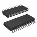 CYW256OXCT
The activity of extra discounts on wholesale prices is in full swing…
Please fill in your contact information and we will send you the latest wholesale price list.





